Qualcomm Demos 48-Core Centriq 2400 Server SoC in Action, Begins Sampling
by Anton Shilov on December 16, 2016 6:00 PM EST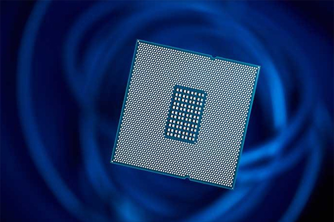
Qualcomm this month demonstrated its 48-core Centriq 2400 SoC in action and announced that it had started to sample its first server processor with select customers. The live showcase is an important milestone for the SoC because it proves that the part is functional and is on track for commercialization in the second half of next year.
Qualcomm announced plans to enter the server market more than two years ago, in November 2014, but the first rumors about the company’s intentions to develop server CPUs emerged long before that. In fact, being one of the largest designers of ARM-based SoCs for mobile devices, Qualcomm was well prepared to move beyond smartphones and tablets. However, while it is not easy to develop a custom ARMv8 processor core and build a server-grade SoC, building an ecosystem around such chip is even more complicated in a world where ARM-based servers are typically used in isolated cases. From the very start, Qualcomm has been rather serious not only about the processors themselves but also about the ecosystem and support by third parties (Facebook was one of the first companies to support Qualcomm’s server efforts). In 2015, Qualcomm teamed up with Xilinx and Mellanox to ensure that its server SoCs are compatible with FPGA-based accelerators and data-center connectivity solutions (the fruits of this partnership will likely emerge in 2018 at best). Then it released a development platform featuring its custom 24-core ARMv8 SoC that it made available to customers and various partners among ISVs, IHVs and so on. Earlier this year the company co-founded the CCIX consortium to standardize various special-purpose accelerators for data-centers and make certain that its processors can support them. Taking into account all the evangelization and preparation work that Qualcomm has disclosed so far, it is evident that the company is very serious about its server business.
From the hardware standpoint, Qualcomm’s initial server platform will rely on the company’s Centriq 2400-series family of microprocessors that will be made using a 10 nm FinFET fabrication process in the second half of next year. Qualcomm does not name the exact manufacturing technology, but the timeframe points to either performance-optimized Samsung’s 10LPP or TSMC’s CLN10FF (keep in mind that TSMC has a lot of experience fabbing large chips and a 48-core SoC is not going to be small). The key element of the Centriq 2400 will be Qualcomm’s custom ARMv8-compliant 64-bit core code-named Falkor. Qualcomm has yet has to disclose more information about Falkor, but the important thing here is that this core was purpose-built for data-center applications, which means that it will likely be faster than the company’s cores used inside mobile SoCs when running appropriate workloads. Qualcomm currently keeps peculiarities of its cores under wraps, but it is logical to expect the developer to increase frequency potential of the Falkor cores (vs mobile ones), add support of L3 cache and make other tweaks to maximize their performance. The SoCs do not support any multi-threading or SMP technologies, hence boxes based on the Centriq 2400-series will be single-socket machines able to handle up to 48 threads. The core count is an obvious promotional point that Qualcomm is going to use over competing offerings and it is naturally going to capitalize on the fact that it takes two Intel multi-core CPUs to offer the same amount of physical cores. Another advantage of the Qualcomm Centriq over rivals could be the integration of various I/O components (storage, network, basic graphics, etc.) that are now supported by PCH or other chips, but that is something that the company yet has to confirm.

From the platform point of view, Qualcomm follows ARM’s guidelines for servers, which is why machines running the Centriq 2400-series SoC will be compliant with ARM’s server base system architecture and server base boot requirements. The former is not a mandatory specification, but it defines an architecture that developers of OSes, hypervisors, software and firmware can rely on. As a result, servers compliant with the SBSA promise to support more software and hardware components out-of-the-box, an important thing for high-volume products. Apart from giant cloud companies like Amazon, Facebook, Google and Microsoft that develop their own software (and who are evaluating Centriq CPUs), Qualcomm targets traditional server OEMs like Quanta or Wiwynn (a subsidiary of Wistron) with the Centriq and for these companies having software compatibility matters a lot. On the other hand, Qualcomm’s primary server targets are large cloud companies, whereas server makers do not have their samples of Centriq yet.
During the presentation, Qualcomm demonstrated Centriq 2400-based 1U 1P servers running Apache Spark, Hadoop on Linux, and Java: a typical set of server software. No performance numbers were shared and the company did not open up the boxes so not to disclose any further information about the CPUs (i.e., the number of DDR memory channels, type of cooling, supported storage options, etc.).
Qualcomm intends to start selling its Centriq 2400-series processors in the second half of next year. Typically it takes developers of server platforms a year to polish off their designs before they can ship them, normally it would make sense to expect Centriq 2400-based machines to emerge in the latter half of 2H 2017. But since Qualcomm wants to address operators of cloud data-centers first and companies like Facebook and Google develop and build their own servers, they do not have to extensively test them in different applications, but just make sure that the chips can run their software stack.
As for the server world outside of cloud companies, it remains to be seen whether the server industry is going to bite Qualcomm’s server platform given the lukewarm welcome for ARMv8 servers in general. For these markets, performance, compatibility, and longevity are all critical factors in adopting a new set of protocols.
Related Reading:
- Evaluating Futuremark's Servermark VDI on the Supermicro SYS-5028D-TN4T
- New GIGABYTE Server Motherboards Show Xeon D Round 2
- AMD Exits Dense Microserver Business, Ends SeaMicro Brand
Source: Qualcomm


88 Comments
View All Comments
webdoctors - Sunday, December 18, 2016 - link
Ya I was going to add the same point. The Sun Niagara series of processors has been around for almost a decade now and its got tons of weak cores for running many web server threads.Also, as others have pointed out, the decoder logic is small dynamic power overhead compared to the static cache and out of order dynamic power, so ARM cores are not blatantly more power efficient than x86 in the high performance realm.
Anyways, more competition is great, and AMD, IBM, Oracle, Intel will have another competitor, consumers will have more choices. I haven't heard of anyone working on ARM cores for HPC and servers, maybe it'll happen but its definitely a pretty niche market at the moment.
FunBunny2 - Sunday, December 18, 2016 - link
-- Also, as others have pointed out, the decoder logic is small dynamic power overhead compared to the static cache and out of order dynamic power, so ARM cores are not blatantly more power efficient than x86 in the high performance realm.what folks are missing is the obvious: X86 is a CISC ISA which is "decoded" to RISC (we don't, so far as I know, know the ISA of this real machine). the ARM "decoder" is along the lines of old transparent machines of the likes of IBM 360: the compiler (COBOL, mostly, in the case of the 360) takes the source, turns it into assembler, which the decoder turns into machine instructions, one-for-one. that's what decoder meant for decades.
Intel (and perhaps others before, I don't know) chose to use those billions and billions of transistors to make a RISC machine on the hardware, hidden behind a "decoder" which is really a hardware JIT CISC -> RISC.
the Intel way leads to simpler compilers which need only spit out legacy X86 assembler (modulo additional instructions, still CISC, that have come along the way), while the ARM compilers have to take that source figure out how to get down to real hardware instructions. so, yes, the object file from an ARM compiler will be bigger and more complicated, but easier to handle at run time. the real issue: which runs faster in the wild; the eventual RISC code in the X86 machine (counting all that decoding/caching/etc.) or the native RISC code in ARM. I've no idea.
Wilco1 - Sunday, December 18, 2016 - link
No, in all cases instructions are decoded by hardware into one or more internal micro-ops which are then executed (so there is no JIT compiler - Transmeta and NVidia Denver are rare exceptions).Both CPUs and compilers prefer simpler instructions since complex instructions are too slow and too difficult to optimize for (this is why RISC originally started). As a result all commonly used instructions are decoded into a single micro-op, both on RISC and CISC CPUs.
The difference is in the complexity, a RISC decoder is significantly simpler and smaller than a CISC one. For example instructions on x86 can be between 1 and 16 bytes long on x86, and each instruction can have multiple prefixes, slightly modifying behaviour. You need a micro code engine for the more complex instructions even if they are very rarely used. On high-end cores you require a stack engine to optimize push/pop operations and a micro-op cache to reduce power and decode latency. All this adds a lot of transistors, power and complexity even on a high-end core.
Writing a compiler backend for a RISC CPU is easier due to the simpler, more orthogonal instructions. RISC doesn't imply larger object sizes either: ARM and Thumb-2 are smaller than x86 and AArch64 is smaller than x64. Why? Unlike RISC, the encodings on x86/x64 are not streamlined at all. Due to all the extra prefixes and backwards compatibility instructions are now over 4 bytes on average. x86 also requires more instructions in various cases due to having fewer registers, less powerful operations and branches.
FunBunny2 - Sunday, December 18, 2016 - link
-- No, in all cases instructions are decoded by hardware into one or more internal micro-ops which are then executed (so there is no JIT compiler - Transmeta and NVidia Denver are rare exceptions).tom-aye-to or tom-ah-to. if the "decoder" has to figure out what instruction stream to emit to the hardware, that's a compiler JIT or otherwise. the mere fact that micro-op caches exist is confirmation that "JIT" is happening.
Wilco1 - Sunday, December 18, 2016 - link
It's only called JIT if the translation is done by software and involves optimization. If it is done by hardware and a fixed expansion for every instruction then it's simply decoding. CPUs have translated their ISA into internal instructions since the early days.Also a micro-op cache has nothing to do with "JIT". Neither do pre-decode caches. Both are signs that decode is so complex that there is an advantage in caching the results. Not necessarily a good sign.
FunBunny2 - Sunday, December 18, 2016 - link
-- CPUs have translated their ISA into internal instructions since the early days.not to be too picky (OK, may be), but in the "early days" decode meant taking the assembler output, machine code instructions, one line at a time, to set the hardware. no substitution or other stuff happened.
the first exception that I know of came with the 360 machines. the top of the line machines executed the ISA directly in hardware, while the /30 had hardware, legend has it, similar to a DEC PDP which was driven by "microcode" equivalent to 360 assembler. the in-between machines had in-between implementation.
deltaFx2 - Sunday, December 18, 2016 - link
"complex instructions are too slow and too difficult to optimize for": Huh? That was circa 1980. Use intel's icc compiler and look at the disassembly. It extensively uses complex addressing modes and ld-op/ld-op-store. In Spec, footprint is easily 20% smaller than gcc.ARM != RISC. See my earlier post, I'm not going over this again.
"Why? Unlike RISC, the encodings on x86/x64 are not streamlined at all. Due to all the extra prefixes and backwards compatibility instructions are now over 4 bytes on average. x86 also requires more instructions in various cases due to having fewer registers, less powerful operations and branches."
See what you did there? Claim: ARM binaries smaller I$ footprint. Reason: x86 has larger instructions. Even if we accept that x86 has larger instructions (not true), if each instruction encodes more information, this is amortized. In typical workloads, x86 ranges between 2-3 (non-vectorized/non-FP). Also remember that x86 allows you to encode 32-bit immediates in the instruction. In ARM, you either have to compute that value, or load it. ARM's largest immediate is 16-bit or less. AVX is larger than 4 bytes, but it supports 256 bit operations.
x86 has fewer registers, but supports ld-op/op-store/ld-op-store. ARM needs a register to load to, before doing the EX. So you need to rename all these temps and keep them around just in case there's an exception. There's no free lunch, mate.
Branches: That's just nonsense. If you're referring to predication, predication is usually a bad idea for an out-of-order CPU, because you have to execute ~2x the number of instructions. It only makes sense if the branches are hard to predict, and x86 has a cmov instruction for that (analogous to csel). ARM relied on predication in A32 as an easy way of avoiding a fancy branch predictor, and stalling the pipeline on a branch. This makes sense in 1990, but not in the market ARM currently competes in.
Wilco1 - Sunday, December 18, 2016 - link
Yes it's well known and widely discussed problem that icc generates too long and too CISCy instructions that stall decode and require pre-rename expansion. Load-op-store is a bad idea on pretty much all x86 CPUs. Load-op helps in some cases as modern cores keep them fused until after rename (and dispatch is now finally 6-wide), however they are not frequently used in compiled code. I did some measurements a while back, load-op was around 5% of loads and the majority of cases were test and cmp. Not exactly "extensive use"."ARM != RISC"??? So you have no idea what RISC means then. Oh well...
Yes, it's a fact that ARM binaries are smaller than x86. x86 both uses larger and slightly more instructions. That includes non-vectorized integer code. Compile some binaries and educate yourself. I did. Note the semantic content of instructions is very close - this means on average each instruction encodes the same amount of information (despite using some load+op or complex addressing modes). x86 just happens to use a less dense encoding.
"So you need to rename all these temps and keep them around just in case there's an exception. There's no free lunch, mate."
And you believe x86 doesn't need extra rename registers for all those temporaries and keep those around too??? No free lunch indeed.
As for predication/CSEL, this is still extensively used on modern cores to improve performance since there are still many hard to predict branches. Executing 1 or 2 extra instructions is far cheaper than a 10% chance of a branch mispredict. The only reason it isn't used much on x86 is because cmov sucks big time on most cores, so x86 compilers typically emit complex sequences of alu instructions for functions like abs, conditional negate etc...
deltaFx2 - Sunday, December 18, 2016 - link
RISC, when the idea was introduced in academia by Patterson et al. meant an ISA in which each instruction executes in a single cycle. Anything longer than that has to be handled in software, so no mul or div or FP instructions. Clearly that wasn't a great idea. So the idea morphed to being multi-cycle ops ok as long as they don't involve multiple ops (in other words, no complex state machine, aka microcode). Except that the push/pop instructions that A32 has requires some sequencer (ucode or h/w is beside the point). As do load with autoincrement, and a host of other instructions in A32 and A64. So what is RISC, according to you? Fixed instruction length? ARM isn't that either (pure 64 bit is, of course). Load-store architecture? That's a pretty tenuous link to the original definition then.Re. CSEL/CMOV, compile hmmer (Spec2006) using gcc O2 and see what you get. I've seen cmov all over the place in x86. As to it sucking, there's no reason it should, but I don't know what intel does. And the hard-to-predict branches are precisely the point. hmmer has a bunch of load->compare->branch sequences that are predicated this way.
Re binary size, that's not my experience. gcc -O2 produced (circa early 2015) pretty large A64 binaries; slightly larger than corresponding x86-64 (dynamic count). I suppose it also depends on your compiler switches. If x86 by default compiles for performance, ARM compiles for code footprint, then that might do it.
Re. ld-op temps, usually you'll keep them until the ld-op retires. In ARM, the temp is held past retire because it's architected state. And you'll have to spill/fill them across function calls, etc. to maintain state, even if it's long dead. At any rate, my point was that x86's ISA allows for more registers than apparent just by looking at the architected state.
Again, your experience of ld-op differs from mine. I've found it to be as high as 30% of loads. Perhaps there's something in your code that requires the loaded value to be kept around in architected state (like 2+ consumers). It's possible, idk.
Not sure why you think ld-op-store is always a bad idea.
Anyways, let's put the ARM vs x86 code size argument down as: "it depends". This is a paper online that suggests x86 is denser or as dense as thumb-2. http://web.eece.maine.edu/~vweaver/papers/iccd09/i... I'm sure a workload that makes heavy use of ARM's autoincremented loads and doesn't allow x86 to use ld-op will yield the opposite result.
name99 - Monday, December 19, 2016 - link
"RISC, when the idea was introduced in academia by Patterson et al. meant an ISA in which each instruction executes in a single cycle."Yes and no. You can read what Patterson et al said in their own words here:
https://courses.cs.washington.edu/courses/cse548/0...
IMHO the IMPORTANT part of this document is the first and second paragraphs.
The complaints against CISC (and thus the point of RISC) are that CISC
- has increased design time
- increased design errors
- inconsistent implementations
- poor use of scarce resources (especially transistors).
To that end RISC
- execute one instruction per cycle. (NOT one cycle instructions! Infeasible even on the very first chip which had two cycle load/store.) This is a pointless restriction that was soon tossed.
- all instruction the same size. (This helps massively. It's what allows Apple to decode 6 instructions per cycle [and IBM to do even more] while to get results worse than that Intel needs a ton of helper machinery, increased every iteration and now consisting of essentially two parallel independent instruction caches.)
- load-store architecture. (This is also essential, in that Intel uses the same thing, through micro-ops)
- only include instructions that can be exploited by high-level languages. (This has been a constantly moving target. It's still not clear to me if the ARM and ARMv8 2/3/4 vector transposition instructions are worth their hassle, and whether real compilers can use them without developers having to resort to assembly.)
All in all I'd say the score-card 35 years on looks like
- same sized instructions (or only two sizes ala ARM+Thumb) is immensely helpful
- load-store is essential, so much so that you fake it if you have to
- one instruction per cycle (or one cycle instructions) is neither here nor there.
- the one BIG omission to the paper is that you don't want instructions that modify various pieces of implicit state (implicit flags for carry or branching or various sorts of exceptions, implicit stack pointer)
- IMHO memory model/memory ordering is a HUGE issue, but it's one of these things that's invisible to anyone outside one of the big companies, so we have no data on how much difficulty it adds.
We do have ONE data point --- that Intel screwed up their first attempt at HW transactional memory, whereas IBM didn't [for both POWER and z-Series which is a CISC that is mostly RISC-like, much more so than Intel]. But maybe IBM was just more careful --- we have to wait to see how the various ARM company's attempts to implement the more sophisticated memory semantics of ARMv8.1 and v8.2 [and eventually transactional memory] go.
- short term decisions to save a few transistors are stupid no matter who does them. Intel did this all over the place (and not just at the start *cough* MMX *cough*). MIPS did it with delayed branch slots. ARMv8 seems to have done remarkably well in this respect with nothing that I can think of that screams "stupid short-sighted idea". (Some would say the effective limitation to 56 address bits is such. We shall see. Perhaps five years from now we'll all be using the new Vector extensions, and at that point Neon will seem like a bad idea that the designer all wish they could strip from the ISA?)
"In ARM, the temp is held past retire because it's architected state. And you'll have to spill/fill them across function calls, etc. to maintain state, even if it's long dead. "
Not exactly true. Yes, the HW has to commit these temporary register writes, but commit is off the critical path.
But in most cases the calling conventions define volatile and non-volatile registers so, no, you do NOT have to spill and fill registers that are just temporaries, not unless you're using unusually large numbers of them in unusual ways.
Oh, one more thing, what's with the constant reference to 32-bit ARM? No-one in the server space (or in the "anything larger than a watch" space --- and let's see how long it is till the Apple Watch switches to ARMv8; my guess is by 2020 at the latest) gives a damn about 32-bit ARM.
Argue about relevant design decisions, not about choices that were a big deal back in 2003!