AMD's Future in Servers: New 7000-Series CPUs Launched and EPYC Analysis
by Ian Cutress on June 20, 2017 4:00 PM EST- Posted in
- CPUs
- AMD
- Enterprise CPUs
- EPYC
- Whitehaven
- 1P
- 2P
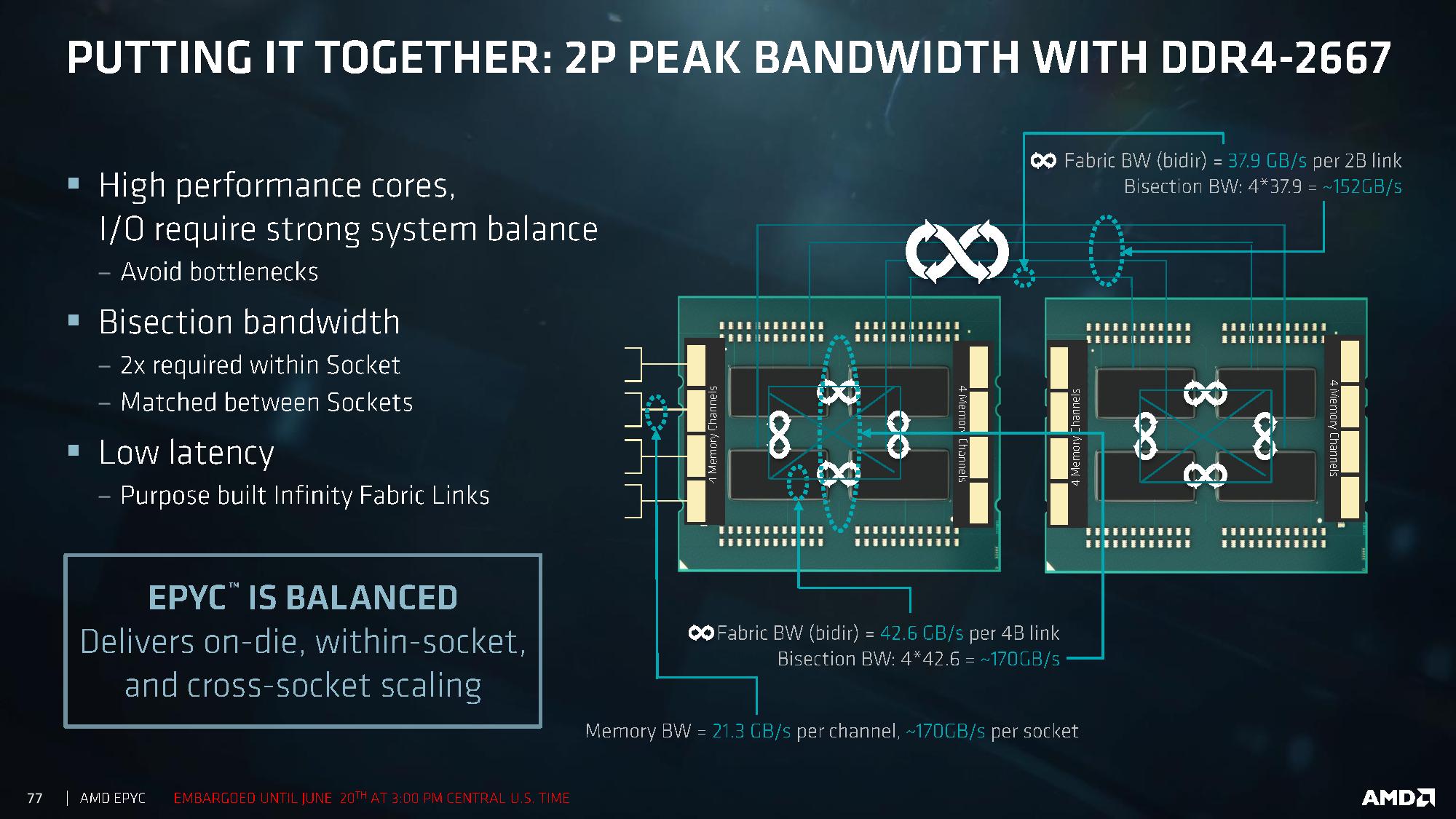
NUMA NUMA IEI: Infinity Fabric Bandwidths
The news about AMD using four Zeppelin dies from Ryzen to form EPYC is not new news, having been shown several times before. However, given the design of the silicon and how the cores communicate, there has been a few worries about how the intra-package communications will be affected by not being a single monolithic die. Beyond that, socket-to-socket communications can also be an issue without sufficient latency and bandwidth.
In a single monolithic die, the latency to access other cores is usually a predictable average, with a regular latency and bandwidth out to the memory channels. Because EPYC has two memory channels per die, if a core needs to access DRAM associated with another die, it adds additional hops and latency to the access, slowing down potential instruction throughput. In the land of dual socket systems, this is known as NUMA: Non-Unified Memory Architecture. The way around a NUMA environment is data locality – keeping the data that a core needs as close as feasibly possible. Solving NUMA is a difficult task, and attempted both at the silicon and software level. Most high-end professional software packages designed for dual-socket systems are NUMA aware, and are designed to compensate for this. The majority of non-high-end software though, is not.
Intra-Socket
With the quad-die design, a single EPYC processor might essentially have four zones for NUMA to occur, based on communication paths. AMD went to specifically address this issue in their design briefings.
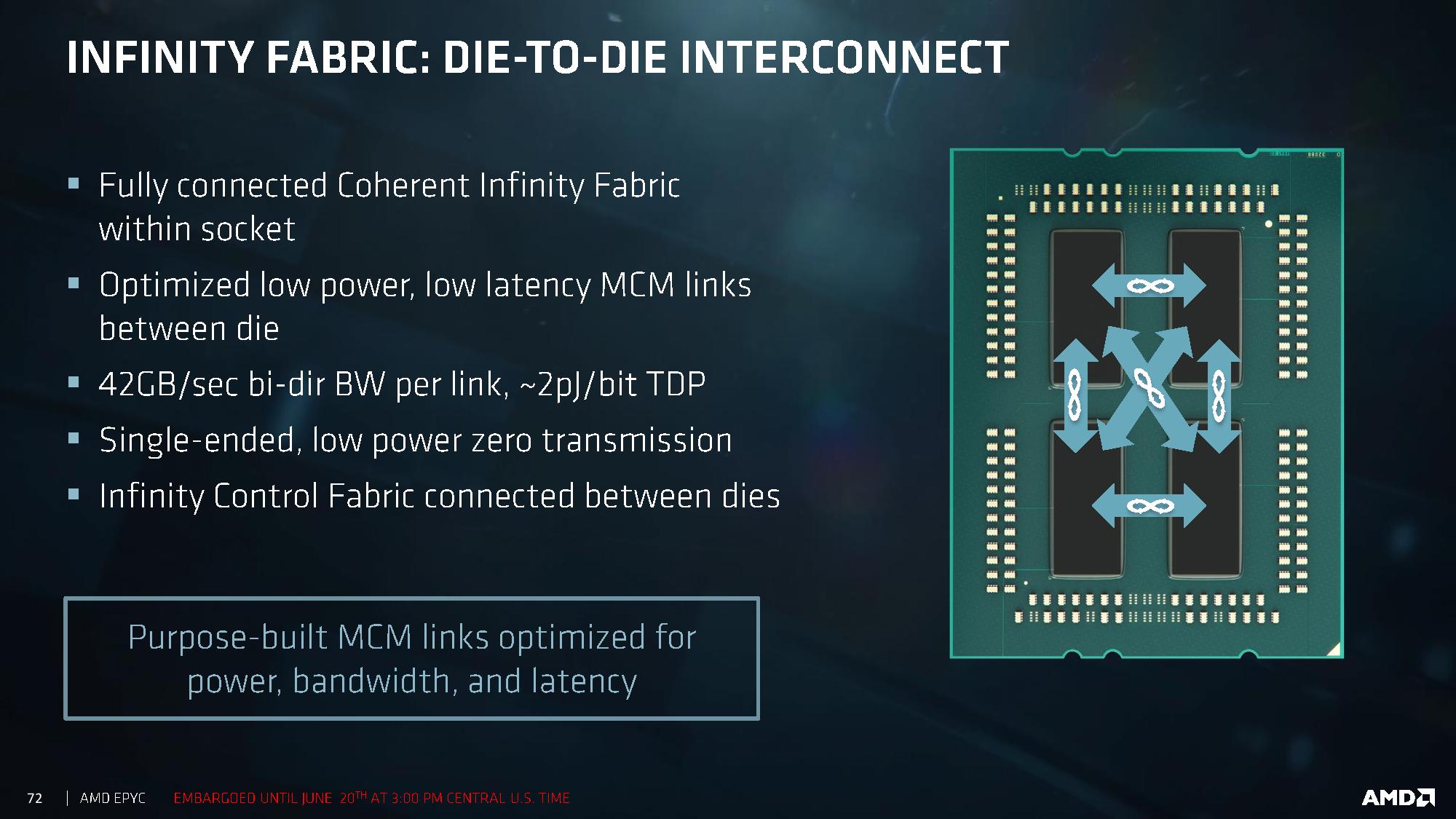
Within a single processor, each of the three dies is directly linked to each other through the Infinity Fabric, so only one hop is ever needed when data goes off-die. The connectivity here is set at a bidirectional 42.6 GB/sec per link, at around an average energy of ~2 pJ per bit (or 0.672W per link, 0.336W per die per link, totaling 4.032W for the chip). It is worth noting that Intel’s eDRAM for Broadwell was set as a 50 GB/s bidirectional link, so in essence moving off die in EPYC has a slightly slower bandwidth than Crystalwell. With a total of six links within the silicon, that provides a total of 2 terabits per second of data movement, although AMD didn’t state what the bottlenecks or latency values were.
Inter-Socket
Socket-to-socket communication is designed at the die level, rather than going through a singular interface. One die in each processor is linked to the same die in the other processor, meaning that for the worst-case scenario data has to make two hops to reach a core or memory controller on the other side of the system. Each link has a bidirectional 37.9 GB/s bandwidth, which is only slightly less than the intra-socket communication bandwidth, although we would expect socket-to-socket to have a slightly higher latency based on distance. AMD has not shared latency numbers at this time.
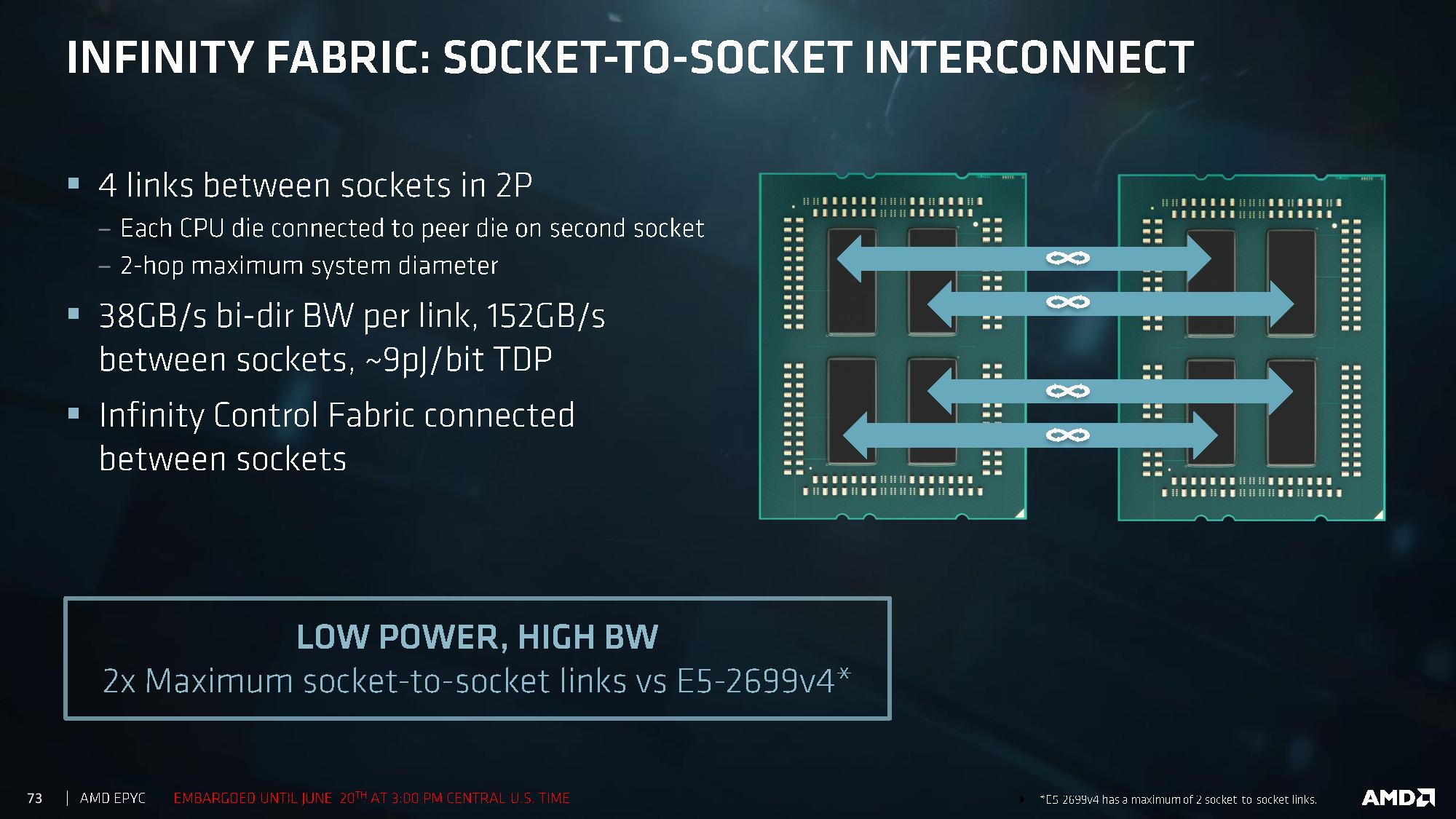
At 37.9 GB/s per link, this totals 152 GB/s between sockets, which AMD states runs at an average of 9 pJ per bit. So at full speed, this link will consume 10.94W between the two sockets, or 5.48W per processor and 1.368W per silicon die.
Totaling the 1.368W per die for socket-to-socket plus 3*0.336W per die for intra-socket communications, the Infinity Fabric can consume 2.376W per silicon die on average when going at full speed.
Infinity Fabric Latency
AMD has not provided Infinity Fabric numbers for latency. We are waiting on information, but this is likely going to be a critical answer for some software packages. Based on testing done by PC Perspective, we already know some latency numbers within a single Zeppelin die from the Ryzen platform. This allows us to fill in the following table showing how long it takes to ping another core:
| EPYC (Naples) Thread Ping Connections | ||
| Latency | Bandwidth | |
| Within A Core | 26 ns | - |
| Core-to-Core, Same CCX | 42 ns | - |
| Core-to-Core, Different CCX, Same Die | 142 ns | - |
| Die-to-Die, Same Package | ? | 42.6 GB/s |
| Die-to-Die, Different Socket, One Hop | ? | 37.9 GB/s |
| Die-to-Die, Different Socket, Two Hops | ? | 37.9 GB/s |
| Core to DRAM, Same Die | ? | 42.6 GB/s |
| Core to DRAM, Different Die | ? | 42.6 GB/s |
| Core to DRAM, Different Socket, One Hop | ? | 37.9 GB/s |
| Core to DRAM, Different Socket, Two Hops | ? | 37.9 GB/s |
PCIe Bandwidth
Each Zeppelin die can create two PCIe 3.0 x16 links, which means a full EPYC processor is capable of eight x16 links totaling the 128 PCIe lanes presented earlier. AMD has designed these links such that they can support both PCIe at 8 GT/s and Infinity Fabric at 10.6 GT/s, although in PCIe mode this means 32GB/s of bidirectional bandwidth per link, suitable for 256GB/s per socket. One of AMD’s proposed benefits here is link bifurcation support:
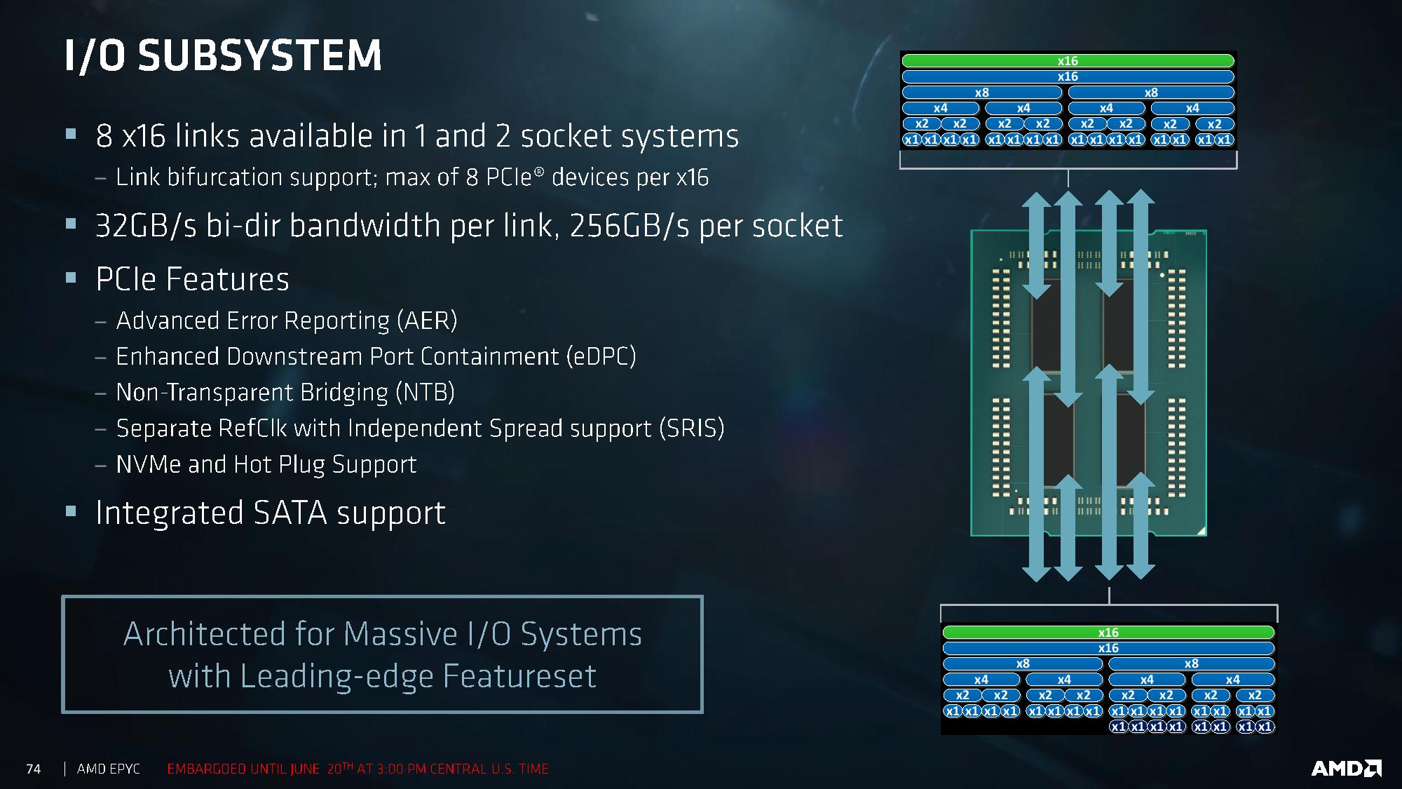
Each x16 link can support Infinity Fabric (green), PCIe (blue) and SATA (dark blue). PCIe can be bifurcated all the way down to sets of x1, although there will be a limit of 8 PCIe devices per x16 link, but this becomes a mix and match game: x8 + x4 + x2 + x1 + x1 + x1 + x1 becomes entirely valid for a single x16 link, and each CPU has eight of these such links. For the SATA connectivity, each x16 link can support 8 SATA drives as a result. If you really want 64 devices per processor, welcome to your platform without buying PCIe switches. AMD states that as an NVMe implementation, supporting 32 NVMe devices is going to be no sweat for an EPYC system.
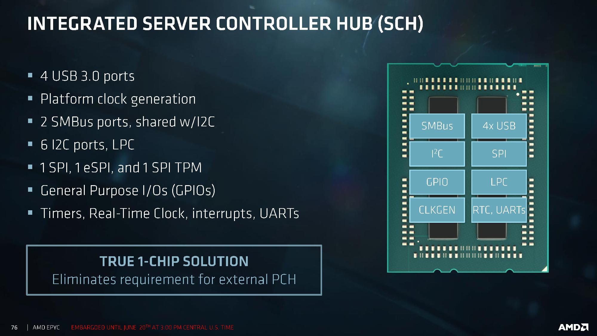
This also relates to the Sever Controller Hub, which acts as part of the design offering four USB 3.0 ports, SMBus, I2C, SPI, eSPI, TPM, GPIOs, timers and UARTs.
Combining The Bandwidth
Altogether, AMD is stating that they are relatively unconcerned about NUMA related issues, with bandwidth between dies and between sockets being relatively similar. It is worth noting that the 42.6 GB/s die-to-die bandwidth is identical to the dual-channel memory bandwidth quoted per die:
Time will tell if these become bottlenecks. Latency numbers please, I’d love to fill in that table above.


131 Comments
View All Comments
davegraham - Tuesday, June 20, 2017 - link
I'm waiting to see consumer sites benchmark a server CPU against retail CPUs and then crow about clocks, etc. ;) it'll be done, it'll be vicious, and people will take it as the gospel truth. heck, let's just get the Cinebench testing done ASAP and call it day ;)Gothmoth - Tuesday, June 20, 2017 - link
yeah why is anandtech reporting about server hardware. nobody is interested in that.just let us take AMDs numbers as gospel.... a interpolate threadripper numbers until august.
SkiBum1207 - Tuesday, June 20, 2017 - link
Excuse me? There are us who use servers to make money - we definitely care about Anandtech's analysis of enterprise hardware.davegraham - Tuesday, June 20, 2017 - link
I am interested in Ian's take but I test this hardware on my own using the toolsets available to me. While I appreciate Johan's insights, I find most of the consumer sites (as Anandtech is one of them) to be reaching when they try to provide realistic workload testing. StorageReview.com does a decent job (mostly), but I'm finding that most reviews, sadly, are hit and miss against test benches and their applicability is...dubious at best.and like LurkingSince97 infers, spec-int is a fanboy benchmark ;)
D
at80eighty - Tuesday, June 20, 2017 - link
did you discover the site yesterday?davegraham - Tuesday, June 20, 2017 - link
lol. who, me? nope. ;)at80eighty - Wednesday, June 21, 2017 - link
sorry, the comment threading is not helpful - i directed that question to Gothmoth's absurd postdeltaFx2 - Wednesday, June 21, 2017 - link
Plenty of people are interested in it, and those people do their own benchmarking. They don't visit Anandtech or Tom's hardware to get this information.LurkingSince97 - Tuesday, June 20, 2017 - link
Except that nobody runs spec-int on their servers.AMD made two mistakes:
1. spec-int should not be used to compare servers across architectures. Instead, run real software that people use on servers. Virtualization benchmarks, JVM stuff, databases, whatever. Real world things.
2. Trying to modify spec-int results (I guess, by using GCC instead of intel's compiler, and compensating for the stuff their compiler does). Yeah, a lot of the tricks that some compilers use on spec-int are absolutely garbage and would not make real-world applications faster -- just spec-int. But there is no objective way to disentangle that. So stay away from it.
IanHagen - Tuesday, June 20, 2017 - link
Intel's compiler cripples code on AMD and VIA chipsAnti-competitive at the machine code level
https://www.theinquirer.net/inquirer/news/1567108/...
Intel finally agrees to pay $15 to Pentium 4 owners over AMD Athlon benchmarking shenanigans
https://www.extremetech.com/computing/193480-intel...
FTC Settles Charges of Anticompetitive Conduct Against Intel
https://www.ftc.gov/news-events/press-releases/201...