Samsung Starts Production of HBM2 “Aquabolt” Memory: 8 GB, 2.4 Gbps
by Anton Shilov on January 11, 2018 1:45 PM EST
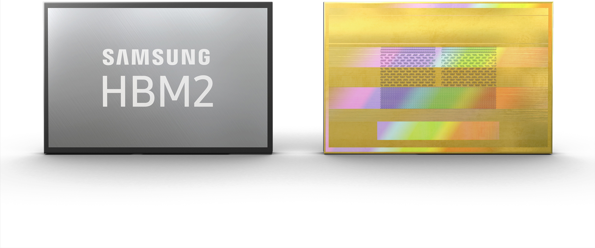
Samsung this week announced that it had started mass production of its second-generation HBM2 memory code-named “Aquabolt”. The new memory devices have 8 GB capacity and operate at 2.4 Gbps data rate per pin. To hit the new data rate, Samsung had to apply new technologies related to TSV design and thermal control. Samsung intends to offer the new memory to customers for use in next-gen HPC, AI and graphics solutions.
General architecture of Samsung’s new 8 GB HBM2 “Aquabolt” memory is similar to the company’s previous-gen 8 GB HBM2 “Flarebolt” devices: each KGSDs (known good stacked die) is comprised of eight 8-Gb memory ICs (integrated circuits) interconnected using TSVs (through silicon vias) in an 8-Hi stack configuration. Every KGSD features a 1024-bit bus and with a 2.4 Gbps per pin data rate, it can offer up to 307.2 GB/s of memory bandwidth per stack.
| Samsung's HBM2 Memory Comparison | |||||||
| Aquabolt | Flarebolt | ||||||
| Total Capacity | 8 GB | 8 GB | 4 GB | 8 GB | 4 GB | ||
| Bandwidth Per Pin | 2.4 Gb/s | 2 Gb/s | 2 Gb/s | 1.6 Gb/s | 1.6 Gb/s | ||
| Number of DRAM ICs per Stack | 8 | 8 | 4 | 8 | 4 | ||
| DRAM IC Process Technology | 20 nm | ||||||
| Effective Bus Width | 1024-bit | ||||||
| Voltage | 1.2 V | 1.35 V | 1.2 V | ||||
| Bandwidth per Stack | 307.2 GB/s | 256 GB/s | 204.8 GB/s | ||||
When JEDEC published the HBM2 specification about two years ago, the spec only discussed three different speed bins for this type of memory —1 Gbps, 1.6 Gbps and 2.0 Gbps at 1.2 V for core and I/O — in context of timing parameters. Manufacturers are free to offer other speed bins and then developers of actual products can clock HBM2 memory in accordance with their own requirements for performance and power consumption. Meanwhile, standard HBM2 packages are offered with 1.6 Gbps and 2.0 Gbps speed bins (their actual clocks are 800 MHz and 1 GHz, respectively). It is noteworthy that to hit 2 Gbps, Samsung had to increase HBM2 voltages to 1.35 V, which is beyond what the spec allows, but so are realities of mass production.
Samsung’s new Aquabolt products operate at 2.4 Gbps, which is higher than the standard was designed for. Meanwhile, it seems that all the other parameters of the new HBM2 “Aquabolt” memory are perfectly within the spec. Moreover, Samsung’s new memory even lowers its voltage back to 1.2 V as a result of internal optimizations.
To increase actual memory frequency to 1.2 GHz and decrease voltage to 1.2 V at the same time, Samsung had to apply a new method to reduce collateral clock interference between the 5000+ TSVs. Samsung says that to lower the clock skew it had to decrease the deviation of data transfer speeds among the TSVs, but does not go beyond that. In addition, the company increased the number of thermal bumps between the DRAM dies to distribute heat more evenly across each KGSD and thus better dissipate it. Finally, Samsung’s Aquabolt HBM2 products feature an additional protective layer at the bottom to increase the physical strength of the package. It is unknown whether the strengthening had an impact on mechanical characteristics of KGSDs, but this is a possibility.
Makers of memory usually announce mass production of new DRAMs after they complete production the first batch, so the HBM2 Aquabolt memory from Samsung might already exist in more or less mass quantities. Now, it is up to Samsung’s partners to use the new KGSDs in their products.
It is noteworthy that SK Hynix also has 2.4 Gbps HBM2 chips slated for Q1 availability in its product catalog. It is up to SK Hynix to make appropriate announcements, but it looks like Samsung is not going to be alone with fast HBM2 packages in the coming months.
Related Reading:
- Samsung Increases Production Volumes of 8 GB HBM2 Chips Due to Growing Demand
- JEDEC Publishes HBM2 Specification as Samsung Begins Mass Production of Chips
- SK Hynix: Customers Willing to Pay 2.5 Times More for HBM2 Memory
- Hot Chips 2016: Memory Vendors Discuss Ideas for Future Memory Tech - DDR5, Cheap HBM, & More


Source: Samsung


17 Comments
View All Comments
DanNeely - Thursday, January 11, 2018 - link
It'll be interesting to see if this shows up anywhere at its rated speed. Neither AMD or NVidia have managed to get HBM2 at 2ghz into anything yet.Dragonstongue - Thursday, January 11, 2018 - link
no kidding...maybe heat was the issue, or like most things, the maker in this case samsung is claiming numbers that are simply under the "best case scenario" not in an actual on product (GPU-CPU completed model) or I suppose, maybe AMD and now Nv decide to use a slower clocked variant at lower voltage so as reduce cost to THEM to maximize revenue?Who knows, what I do know, the memory makers need stop being foolish and give the manufacturing capacity to keep end consumer pricing in check, very few DRAM/Flash makers out there, not hard for them to be in collusion i.e drive the price up massively benefits them and royally screws the end customer (the ones they sell it to) or at the very least screws us the consumer...the whole point of DDR to DDR2 etc and a smaller node was to keep pricing in check reduce heat/power, performance going up.
They seem to have gotten the memo on the reduce heat/power, not so much on the first and hit and miss on the 3rd point ^.^
philehidiot - Saturday, January 13, 2018 - link
I'm probably too late to this comment party to get a reply but if any of you uber nerds out there have an opinion on this I'd be interested to hear it.I have 12GB of DDR3 in my system which is mostly used for gaming, web browsing, etc. Occasionally I do some video editing but it's not often enough to warrant more RAM. I have not noticed any issues relating to RAM bottlenecking performance (that's more likely to be down to the ageing but still competent GTX 780).
Given a RAM upgrade to DDR4 would cost me a new mobo, probably a new CPU (especially given it's one that Intel has warned their bug patching will affect considerably) as well as the RAM, does anyone think it's actually worth it? I personally can not see a reason to upgrade it but does anyone think it's going to be holding things back? The DDR3 is running at 1600MHz.
SilthDraeth - Saturday, January 13, 2018 - link
No need to upgrade to more RAM or DDR4 unless you are upgrading your whole system, which you already pointed out. Upgrading you will of course get performance enhancements, but only you know if the money you spend is worth the performance increase you receive.BurntMyBacon - Monday, January 15, 2018 - link
As far as amount, you have plenty of RAM for gaming, web browsing. As far as your RAM speed goes, it is not likely holding you back any more that the CPU it is paired with. This is particularly true if you have triple channel memory. I would suggest your money is much better spent upgrading your still competent, but no longer exceptional GTX780. The GTX780 is a little short on VRAM for the newest games at high resolutions as well. It is possible that a particularly low end or very old processor and/or a lower resolution monitor (you didn't specify these) will place the bottleneck on the CPU, but it is less likely and RAM is still unlikely to be the issue. Also keep in mind that at this point it looks like gaming performance loss is usually around 3% with a single outlier of around 9%. If you play mostly CPU bound games (I.E. RTS at low resolution), then you may want to consider this. Your safest bet is to simply wait for the patch and play your favorite games. If they don't feel much different, then don't worry about the CPU (from a gaming perspective).Video editing might possibly suffer with the new security patch. It depends on how IO intensive your software / projects are as well as how fast the storage is. Faster storage (I.E. NVME SSD) will see a larger hit while the hit to HDDs may not be noticeable in this scenario. This won't be related to RAM, though.
Santoval - Thursday, January 11, 2018 - link
I suppose you rather mean 2 Gbps (clocked at 1 Ghz), right? It's possible that there were serious TDP and/or power consumption issues with the Flarebolt dies, since they were effectively overclocked. Samsung raised the voltage above spec to 1.35 V, so the power and thermal budget probably went through the roof, as always happens when you raise voltages. However Samsung's new 2.4 Gbps dies went back to 1.2 V, so this time there will be no TDP and power issues. The Aquabolt dies are both much faster and markedly more power efficient. If SK Hynix's 2.4 Gbps dies are in the ~1.35 V range they are probably toast.Santoval - Thursday, January 11, 2018 - link
p.s. I checked the linked pdf of SK Hynix. Their 2.4 Gbps dies are also voltaged at 1.2 V, both their 4- and 8-stack. That's good, because it means that there will be healthy competition and 2.4 Gbps HBM2 prices will not go through the roof.btb - Thursday, January 11, 2018 - link
Would it be possible to put something like this on top of a regular Intel CPU? 1.2 TB memory bandwidth would be pretty insane. Although I'm not sure it will matter for regular usage like gaming?Elstar - Thursday, January 11, 2018 - link
Intel's Xeon Phi product line has 16 GiB of high-bandwidth "MCDRAM" in addition to normal memory.ianmills - Thursday, January 11, 2018 - link
The new Intel chip with radeon graphics has HBM on the package but as a separate die. It that what you mean?