The Western Digital WD Black 3D NAND SSD Review: EVO Meets Its Match
by Ganesh T S & Billy Tallis on April 5, 2018 9:45 AM EST- Posted in
- SSDs
- Storage
- Western Digital
- SanDisk
- NVMe
- Extreme Pro
- WD Black
The Western Digital NVMe Architecture - NAND & Controller
The most interesting aspects of the WD Black 3D NAND SSD come from the new in-house SSD controller and, for the first time, the usage of the 64-layer BICS 3D NAND in one of their retail NVMe SSDs. The 64-layer 3D NAND (BiCS 3) is SanDisk/Toshiba's third-generation 3D NAND. The first two generations had 24 and 48 layers respectively, but saw extremely limited release and neither generation was manufactured in quantities sufficient to displace Toshiba/SanDisk 15nm planar NAND. The production of the 64-layer version is now fully ramped up, and we saw Western Digital use it in the SanDisk Ultra 3D and WD Blue 3D SATA SSDs late last year.
As a refresher, BiCS uses a charge-trap, stacked design that alleviates almost all shortcomings of planar NAND. Bit density can increase from one 3D generation to the next, thanks to predictable scaling in both vertical and lateral dimensions. Availability of a greater number of electrons per NAND cell in the charge trap design compared to planar NAND's floating gate design (at very small geometries) ensures that the reliability and endurance of a 3D NAND cell is almost always better than that of leading-edge planar NAND. The downside is the substantially higher capital investment required to upgrade the 2D NAND producing fab equipment to manufacture 3D NAND wafers.

BiCS 4 (96-layer) is also ramping up production. Most of the 3D NAND volume from Western Digital this year is expected to be the 64-layer BiCS 3 NAND, which is what we see in the WD Black 3D NAND SSD that is being reviewed today.
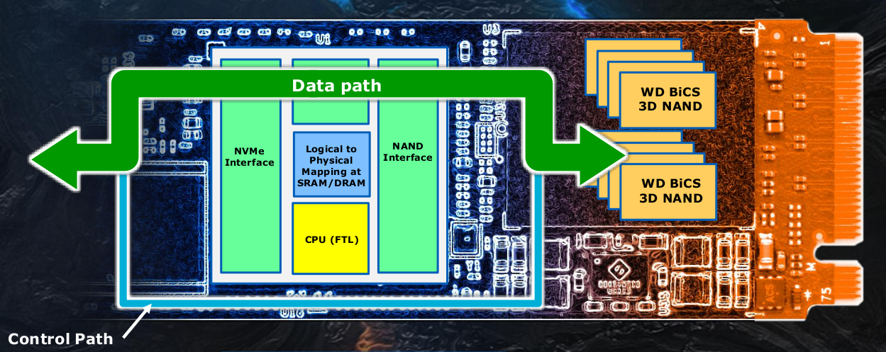
On the controller front, Western Digital has opted to move from a Marvell solution to an in-house design. The primary reason cited was that they could create an architecture that was optimized for BiCS flash - in particular, the controller wouldn't need to support NAND from other vendors, and, the controller could be architected with the future plans for the BiCS line in mind. This makes sense from a flagship perspective - NVMe SSDs push the performance limits, and it is essential to be able to extract every last bit of performance possible from the available NAND. It is no surprise that almost all flash vendors have their own controller for their flagship NVMe SSDs - Samsung uses its own controllers across all its SSDs and Intel uses its own controller for the SSD 900p (Optane). Even mainstream and low-end SSDs from top tier vendors (using merchant controller silicon) come with firmware customized in-house. Vertical integration (starting from flash fabrication and IC assembly to system integration in the form of NVMe or SATA SSDs) allows vendors to optimize performance for their customers.
The new controller has a tri-core architecture (probably using Arm Cortex-R cores) fabricated in a 28nm process. It is designed to be scalable - the current controller can interface with the host using a PCIe 3.0 x4 link, or an x2 link as in the Western Digital SN520. The architecture of the controller also allows future products using variants to come to market faster and with newer features. It also allows Western Digital to segment their NVMe product stack. The controller in the Western Digital Black 3D NAND SSD is optimized for client workloads including PC gaming and high-performance commercial applications. Western Digital expects this new controller architecture to last at least until NVMe SSDs move beyond PCIe 3 x4 interfaces.
Compared to other NVMe SSD controllers that come with a large number of CPU cores, Western Digital is relying less on firmware and more on hardware accelerators to perform the host-to-flash communication (NVMe command processing and data transfer from flash to the host). Power and thermal management tasks are also done without the aid of the CPU cores. The firmware is used only for selective command processing (such as fetching of S.M.A.R.T details, the flash translation layer (FTL) algorithm, and handling exceptions). Avoiding the CPU for all the performance-critical tasks is a means to ensure that the controller is not power hungry.
The WD NVMe SSD Architecture also implements tiered caching (nCache) to improve performance. The WD Black 3D NAND NVMe SSD uses nCache 3.0, which appears to include a host of updates over nCache 2.0.
Prior to going into the details, it is interesting to take a look at how nCache has evolved over the years. In its first generation, nCache was designed to cache the NAND mapping table and small writes (less than 4KB) in a SLC segment on the die. In the second version (first introduced in the SanDisk Ultra II), we saw the move to cache writes of all sizes in the SLC segment first. The size of the SLC cache was also increased to 5GB for every 120GB of user space. nCache 2.0 also implemented an on-chip-copy for the folding mechanism (migrating data from the SLC cache to the main TLC area) that freed up the controller from managing the data-heavy portions of the nCache operations. nCache 2.0 also placed the NAND mapping table in the SLC cache area. The end result being that nCache 2.0 had to route all writes through the SLC cache; this affected sustained write performance greatly, because the SLC cache had to be flushed out to the TLC segment before newer data could be written to it.
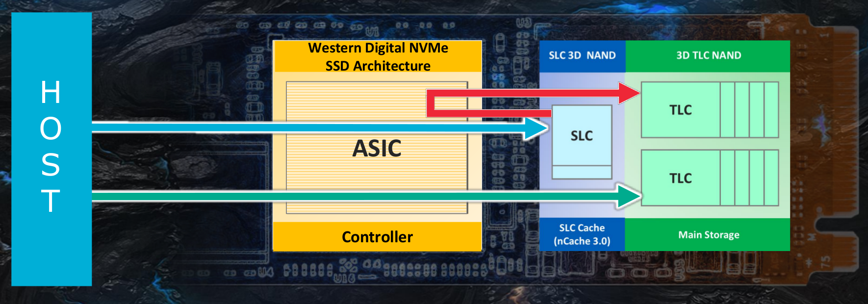
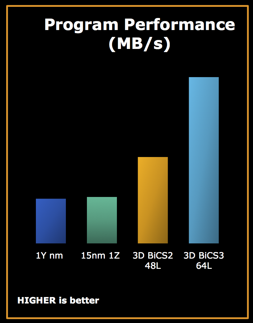
Meanwhile for current-generation products, the performance of 3D TLC is much better than planar TLC when it comes to sustained writes. The endurance is better as well. As a result, rather than sending everything through the SLC cache as with nCache 2.0, nCache 3.0 allows writes to go directly to the TLC space after exhaustion of the SLC segment.
The migration of data from the SLC cache to TLC blocks is performed mostly when the drive is idle, unless the host operating system uses the non-operational power state permissive mode feature of NVMe 1.3 to request that the drive defer background processing. That said, the evacuation policy is aggressive in order to maintain high availability of the SLC blocks. This causes the SSD to perform more writes than it would if data was kept in the cache longer, but Western Digital is confident that their flash has sufficient endurance.
Another major departure from nCache 2.0 seems to be the absence of the on-chip-copy feature available in the previously-used planar TLC dies. Given that 3D TLC allows for direct access during sustained writes, the on-chip-copy feature for folding purposes is not needed.
Finally, Western Digital's nCache 3.0 still uses a fixed size SLC cache, which saves the drive the trouble of converting blocks between SLC and TLC usage. Western Digital has not disclosed the SLC cache sizes for the WD Black, but it appears that our 1TB samples have about 20GB of SLC cache.
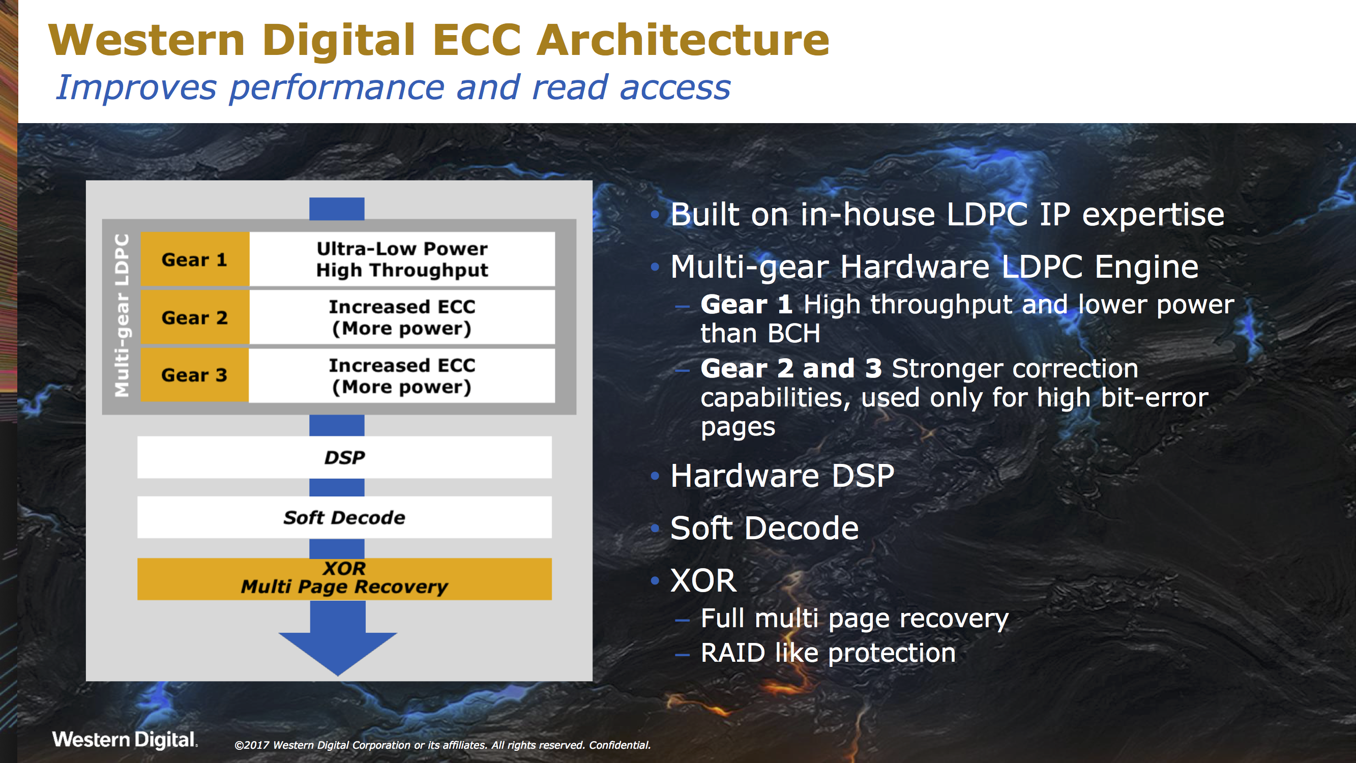
Like any good modern SSD controller, Western Digital's new architecture features multiple layers of error correction. The first three layers are different LDPC-style error correction codes for handling increasing bit error rates, which come at the cost of increasing power consumption and decreased performance. The base level of error correction is an LDPC code that is tuned to offer higher throughput and with lower power requirements than the BCH error correction that nearly all SSDs used before TLC NAND began to take over the market. This lowest layer of error correction is the only one needed during normal operation for most of the drive's lifespan, and this LDPC engine is responsible for less than 10% of the controller's power consumption. The second and third layers of error correction are intended to handle the increasing error rates of a drive that is nearing the end of its write endurance, and these codes are also entirely handled by dedicated hardware on the controller without taking the performance hit of involving the processor cores.
For handling severe data loss that cannot be recovered by the three layers of LDPC, the controller also performs traditional RAID5-like XOR parity. This can handle the failure of defects affecting multiple NAND pages, but consumer SSDs don't include enough excess flash to survive the complete failure of an entire NAND die. Data integrity is also protected by the use of ECC on all of the controller's SRAM and on the external DRAM.


69 Comments
View All Comments
MajGenRelativity - Thursday, April 12, 2018 - link
Higher capacities can be made available at 2280 by using a double sided drive. As for IOPS performance, that can be calculated fairly easily, and I *think* Anandtech does that (I haven't read this review recently). I'm not sure what you mean about the drivers, or "Warranty period directly calculated based on the Endurance fures"oRAirwolf - Friday, April 13, 2018 - link
I would really love it if Anandtech had some common usage scenario load times for things like a large spreadsheet in Excel or how fast some modern games load. I would also be interested to know about things like Windows load time and time to wake up from sleep or hibernation. From what I have seen, all of these super fast nvme ssds don't really have a lot of impact on typical end-user usage scenarios like for office workers or gamers. I love bleeding edge tech and I always want manufacturers to push the limits of price and performance but it seems to me like a lot of people get wrapped around the axles about SSD performance when something like an 850 Evo and a 960 Pro will have almost identical load times in a game.