Power Stamp Alliance Exposes Ice Lake Xeon Details: LGA4189 and 8-Channel Memory
by Ian Cutress on April 9, 2018 11:42 AM EST
For everyone waiting for Cascade Lake, Intel’s next server Xeon platform, to be launched, noise is being made from the Power Stamp Alliance and its members about the platform beyond Cascade Lake. Alliance member Bel Power Solutions, along with the Power Stamp website, have exposed several details on the Ice Lake Xeon platform.
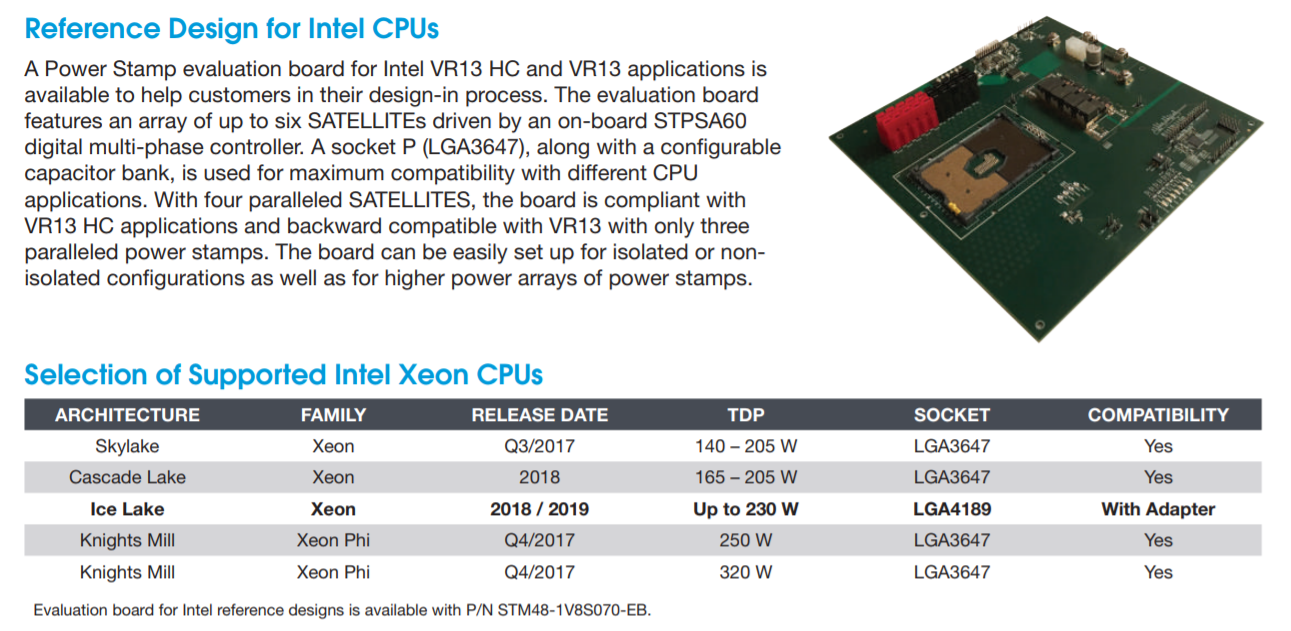
The first element of the information is the new socket, set at LGA4189. This is compared to the current Xeon socket, standing at LGA3647, which currently supports the Skylake Xeon family as well as the upcoming Cascade Lake Xeon family. According to the documents, the power pin implementation between the new LGA4189 and LGA3647 sockets are compatible via an adaptor: this isn’t to say the CPUs themselves will be, but it would appear that all the Skylake/Cascade Lake/Ice Lake Xeon families will have a similar power implementation. The reason why we mention the power implementation only is because the Power Stamp Alliance (and Bel Power Solutions) is only dealing with DC-to-DC converters for the platforms, driving efficiency from a high 48V input correlating with the Open Compute Project (OCP) standards and deployments.

Also in this image (and verified at Power Stamp) are the power ranges for Cascade Lake (165-205W, similar to Skylake Xeons) and for Ice Lake (set to go to 230W). Should the new Ice Lake Xeon platform incorporate features such as OmniPath or on-package FPGAs, which Intel has teased future Xeon platforms to be, then 230W is well within the reasons of possibility. Also, having a high DC-to-DC efficiency is going to assist with overall power consumption and power loss.
Delving into the documents, the Power Stamp Alliance designates two code names in play: VR13 (for Skylake and Cascade Lake) and VR13-HC (for Ice Lake). The HC in this case stands for high-current, and the documentation shows ‘a typical’ VR13-HC implementation with two CPUs and sixteen DDR4 memory slots for each CPU. The Bel Power systems documents goes on to say that a VR13-HC system (Ice Lake) with four power stamps meets the VR13-HC minimum requirements, while only three are needed for VR13 (Skylake/Cascade).
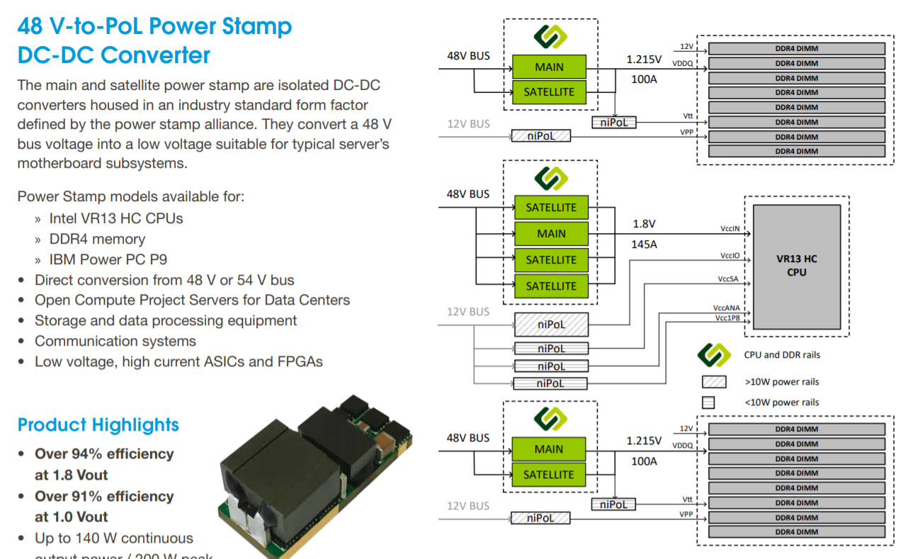
The images shown above and below point to Ice Lake Xeons being equipped with native eight-channel DDR4, given how Intel dropped 3 DIMM per channel support with Skylake. This comes through the chip directly, rather than implementing memory buffers, such as the Jordan Creek implementation on the E7 v4 family. With the 8-channel design, one might assume Intel boosting the maximum memory capacity of the base Xeon processors from 768GB to 1TB, although we should wait to see if that is going to be the case. If Intel is using the same on-chip network implementation as Skylake, it would also mean that one of the segments that previously used for a tri-memory channel controller actually has enough space for a quad-memory channel controller.
No special mention is made regarding XPoint memory support. Parts of the documents state that a set of 8 DRAM slots and two power stamps should be good for 100-200A at 1.215 V for VDDQ, implying that a set of 8 memory sticks should be able to draw around 120W-240W, or ~15-30W each. Varying numbers have been postulated as to the power draw of XPoint modules, but most numbers are within this range.
More information from the Power Stamp Alliance is set to be given at the Open Compute Summit, happening in late May. The Alliance consists of STMicroelectronics, Artesyn Embedded Technologies, Bel Power Solutions, and Flex
Sources: Bel Power Solutions, Power Stamp Alliance, via Twitter
*This article first stated that the OCP Summit was going to happen in Late May. It actually happened in Late March already.


37 Comments
View All Comments
HStewart - Monday, April 9, 2018 - link
What really make EMIB so nice is that it can use different process on the same chip - for example the more critical can be done on smaller processes while less critical like IO can be done on less dense material. Even in example of 980xG even from different manufactures - not just AMD but NVidia also. But the I expect the real use will be Artic Sound GPU implementations in the future. I believe AMD used is only temporary unless GPU or Laptop vendors demand itBut this article sheds light on another possibility up multiple CPUs and include GPU cores on signal modules, What this could main is dual cpu notebooks one day - not just multi-core CPU's
peterfares - Tuesday, April 10, 2018 - link
Dual CPU notebooks wouldn't make much sense unless they're going for more than 18 cores in a single CPU. Maybe in a very long time though.patrickjp93 - Tuesday, April 10, 2018 - link
It would make plenty of sense to save power when not under maximum load.Ian Cutress - Monday, April 9, 2018 - link
As stated, the adapter is likely just to be for translating equivalent power pins. I doubt there's any functionality transfer.edzieba - Tuesday, April 10, 2018 - link
Gaining over 500 pins without any change to footprint and while maintaining power pin layout? That would preclude both a 'use smaller pins' modification (power pins would relocate) or 'use a bigger socket' (would not be drop-in compatible with LGA3647). I wonder if the "Omni Path Stickey-Outey-Bit" will transition from a card-edge protrusion for a separate cable to an additional pinned area.Casper42 - Wednesday, March 4, 2020 - link
I know I'm late to this party, but why not just switch to VCSEL or some other Silicon Photonics option.Effectively have the chip spit out light directly (via interposer or EMIB most likely) and stop messing with Copper Cables.
But since I'm replying from the future, Intel already killed off OmniPath so they don't need to worry about this anymore.
nasfufrsrgiu - Saturday, August 22, 2020 - link
http://bitly.com/zoom-viber-skype-psy