Intel Delays Mass Production of 10 nm CPUs to 2019
by Anton Shilov on April 27, 2018 12:20 PM EST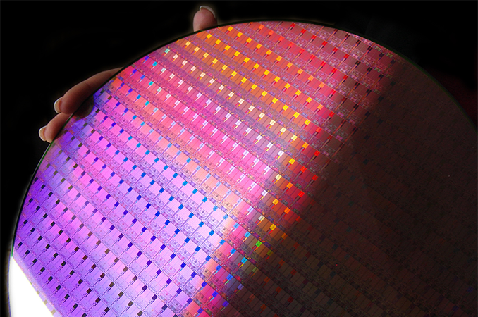
Intel on Thursday announced that it would delay mass production of its 10 nm processors from 2018 to 2019 due to yield issues. The company has claimed to be shipping some of its 10 nm chips in small volumes right now, but due to cost reasons the firm does not intend to initiate their high-volume manufacturing (HVM) at this time. Intel executives also stated that they are confident of their product roadmap and intend to launch Whiskey Lake and Cascade Lake products later this year.
Multipatterning Issues
Brian Krzanich, CEO of Intel, stated during a conference call with financial analysts:
“We are shipping [10-nm chips] in low volume and yields are improving, but the rate of improvement is slower than we anticipated. As a result, volume production is moving from the second half of 2018 into 2019. We understand the yield issues and have defined improvements for them, but they will take time to implement and qualify.”
Intel blames a very high transistor density and consequent heavy use of multipatterning for low yields. Brian Krzanich has said that in certain cases the company needs to use quad (4x), penta (5x), or hexa (6x) patterning for select features as they need to expose the wafer up to six times to “draw” one feature. This not only lengthens Intel’s manufacturing cycle (which by definition rises costs) and the number of masks it uses, but also has an effect on yields.
Intel’s 10 nm fabrication technology relies solely on deep ultraviolet (DUV) lithography with lasers operating on a 193 nm wavelength at this time. The company’s 7 nm manufacturing process will use extreme ultraviolet (EUV) lithography with laser wavelength of 13.5 nm for select layers, eliminating use of extreme multipatterning for certain metal layers. As it appears, right now Intel executives do not consider EUV technology ready for prime time in 2019, so the company’s engineers have to polish off the last DUV-only process (again) rather than jump straight to 7 nm.
10 nm Ramp in 2019
Intel does not elaborate whether it intends to ship (in volume) its 10 nm CPUs in the first half or the second half of 2019, but only says that the company’s engineers know the source of the yield problems and are working hard to fix them. As a result, it is pretty safe to assume that the actual ramp of Intel’s 10 nm production will begin towards the second half of next year.
“We are going to start that ramp as soon as we think the yields are in line, so I said 2019,” Mr. Krzanich noted. “We did not say first or second half, but we will do it as quickly as we can, based on the yield.”
In a bid to stay competitive before its 10-nm CPUs ship in the H2 2019 – H1 2020 (production ramp takes time, bigger processors will launch later than smaller parts), Intel plans to release another generation of products made using its 14 nm process tech. This generation of chips includes Whiskey Lake products for client PCs and Cascade Lake for the datacenter, and both are scheduled for release later this year.
Questions Remain: 10 nm Slip from 2016
Intel’s 10 nm manufacturing process has a long history of delays and without any doubts this transition has been the hardest in the company’s history. Let's do a quick recap.
| Intel First Production |
|
| 1999 | 180 nm |
| 2001 | 130 nm |
| 2003 | 90 nm |
| 2005 | 65 nm |
| 2007 | 45 nm |
| 2009 | 32 nm |
| 2011 | 22 nm |
| 2014 | 14 nm |
| 2016 | |
| 2017 | |
| 2018 | 10 nm? |
| 2019 | 10 nm! |
Intel originally planned to commence shipments of its first processors made using their 10 nm fabrication technology in the second half of 2016. The first rumors about Intel’s problems with the tech started to spread in early 2015 as the company delayed the installation of equipment needed for its 10 nm manufacturing process. Then, in July 2015, the chip giant confirmed intentions to postpone 10 nm HVM from H2 2016 to H2 2017 due to difficulties incurred by multipatterning. Instead, the company promised to release its Kaby Lake products with enhancements and made using a refined 14 nm process (known as 14+ later).
Over the course of 2016 and 2017 we learned that Intel was prepping Cannon Lake (mobile, entry-level desktops), Ice Lake (higher-end client PCs, servers), and Tiger Lake chips on their 10 nm node. We also heard about various problems that Intel faced with its 10 nm technology, but the company refuses to comment on them. The chipmaker did demonstrate a system running a mobile Cannon Lake SoC at CES 2017, with a promise to release this processors late that year. Somewhere along the line, both Ice Lake and Tiger Lake slipped to 2018, which was partly confirmed by the launch of the Coffee Lake CPU made using a revamped 14 nm (14++) in late 2017.
Intel officially introduced the 10 nm fabrication process at IEDM 2017 and said it was on track to start shipments of CNL CPUs in early 2018. In January this year Intel confirmed that they had started to ship Cannon Lake processors in small volumes, but never elaborated. We have since learned that these were CNL-U parts in uninspiring 2+2 and CNL 2+0 configurations, however so far Intel has refused to state who the customer is or where anyone can buy them, despite repeated requests for this information.
Being a very large company, Intel has a multifaceted strategy that spans across product lines and generations. Right now, Intel is battling with yield issues that plague its Cannon Lake product family and the first-gen 10 nm manufacturing process. There are other 10 nm products in the pipeline that are to be made using a refined fabrication technology (such as 10+, 10++). It is pretty obvious that Intel will learn how to improve its 10 nm yields with the CNL lineup, but what remains to be seen is how significantly the delays of this product family affect launch schedules of its successors. Despite Intel's statements, there is outside discussion that Intel could decide to switch right to 7 nm, bypassing 10 nm altogether.
Related Reading
- Intel's 10nm Briefly Appears: Dual Core Cannon Lake in Official Documents
- Intel Mentions 10nm, Briefly
- Intel Displays 10nm Wafer, Commits to 10nm ‘Falcon Mesa’ FPGAs
- Intel at ISSCC 2015: Reaping the Benefits of 14nm and Going Beyond 10nm
Sources: Intel, SeekingAlpha


155 Comments
View All Comments
close - Monday, April 30, 2018 - link
AMD barely touched 50% market share in PCs (you probably mean desktops) at the peak of their popularity during Athlon 64 era - 2006. And the victory was short lived as 2006 was the year Intel launched Core and Core 2. AMD went down to 40% market share in one quarter.Intel knows how to play the game. So even when AMD has the upper hand and the better product Intel knows what to do to stunt their growth by any means necessary (including illegal ones). And they got away with it once so why stop?
willis936 - Saturday, April 28, 2018 - link
Intel’s customers are businesses. Intel’s competitor is a drop in replacement. How are you going to convince a business to spend more on an inferior product? The only path I see is to implement anticompetitive practices to maintain their current customers. You see Nvidia doing it and they don’t even have a remotely threatening competitor.t.s - Saturday, April 28, 2018 - link
With lobbying of course, you silly!t.s - Saturday, April 28, 2018 - link
Agreed. Average Joe is so accustomed with Intel that they 1) never know that competitor exists or 2) still have a negative stigma over AMD, that they don't know how AMD become good competitor in this field now.Yojimbo - Friday, April 27, 2018 - link
"As it appears, right now Intel executives do not consider EUV technology ready for prime time in 2019, so the company’s engineers have to polish off the last DUV-only process (again) rather than jump straight to 7 nm."There are two factors preventing Intel from using EUV in 2019 if they wanted to, or even preventing them from accelerating EUV much more than their current plans in a time frame beyond 2019. Firstly, any such decision needs to be made far in advance. It currently takes ASML 18+ months to fill an EUV tool order. Secondly, ASML only can produce so many EUV machines at a time, owing to Carl Zeiss's ability to produce the optics, and they are already all filled up for 2018 and 2019. So one cannot infer from Intel's lack of EUV usage in 2019 what Intel's current view is on EUV's readiness for prime time, only what their view was 3 years ago, or whenever they were planning out their 10 nm node, and even then only what they though EUV would be ready for at the date they originally planned to be performing high volume 10 nm manufacturing.
p1esk - Friday, April 27, 2018 - link
I'm surprised that this whole EUV ramp up takes such a long time. Given its seeming importance, and the untold billions invested in it, and number of years everyone has been working on it.FullmetalTitan - Friday, April 27, 2018 - link
The complexity of EUV is mind-boggling. There are issue creating the masks because they are many alternating layers. Pelicles are not close to ready and still attenuate too much beam power. Beam power itself was a major hangup, and just with the latest ASML platform hit a level deemed acceptable to foundries buying the tools. Throughput is an order of magnitude slower than DUV/immersion tools. The photoresists are a problem, since you are now using fewer photons with higher energy, shot noise becomes a large problem. Stochastic behaviors throw line edge placement for a loop at small geometries...This list is really a couple pages long but you get the idea.
Yojimbo - Saturday, April 28, 2018 - link
No one bothered putting much effort into the pelicles or the masks until they solved the beam power problem because it could have been wasted effort. People have been confident for a while that the pelicle and mask issues are solvable and will be solved in the time frame necessary. In fact I think ASML says they have them now. At this point the attitude seems to be that EUV is pretty secure. TSMC and other customers (who, I don't know, but probably Intel, Samsung, and GlobalFoundries) have ordered second generation high-NA EUV tools for R&D purposes. The machines cost well over 100 million Euros each. High-NA EUV is not expected to be used until 2023 or 2025 (I forget which). So it seems clear that the foundries are pretty confident in EUV at this moment.From what ASML's CEO said, the reason the ramp takes a long time is because they need to gain experience with the production to assess where to make efficiency improvements. He said it was just the normal engineering learning curve for new manufacturing processes. That's why it takes so much longer at the moment to build an EUV tool than a DUV tool. The reason they can only make 20 EUV tools in 2018 and 30 in 2019 is because Carl Zeiss can only handle producing that many optics systems in those time frames, as they too are learning how to ramp up the EUV optics production. They are already at 0% margins for EUV systems in 2018, I believe. If they tried to push it and produce more they'd be losing money on the additional systems.
p1esk - Saturday, April 28, 2018 - link
Will EUV technology they are developing now be useful or applicable for post-CMOS lithography? Like, I don't know, graphene or photonic circuits?Yojimbo - Sunday, April 29, 2018 - link
I don't know. I think it depends on whatever eventually works out, and what future discoveries are made that lead to that technology winning out. For some technologies they could potentially grow the circuits instead of draw them, in which case photolithography would no longer be the key technology. But, that would demand a major infrastructure shift. Volume manufacture using such a novel method surely is more than a decade out. At the moment, though, I don't think they even have a hopeful candidate to move ahead with. They are still doing basic research on various technologies. The next 10 years of progress will almost certainly rely on photolithography and right now EUV is the only economical way forward. I think there's a good chance, though, that many generations of process nodes will be operated at the same time going forward. Only the projects with fat margins will warrant the die shrinks since the decline in cost per transistor between generations is becoming rather small. So DUV and EUV will exist side-by-side over the next 10 years.