Arm's Cortex-A76 CPU Unveiled: Taking Aim at the Top for 7nm
by Andrei Frumusanu on May 31, 2018 3:01 PM EST- Posted in
- CPUs
- Arm
- Smartphones
- Mobile
- SoCs
- Cortex-A76
Cortex A76 µarch - Backend
Switching to the back-end of the core we have a look at the execution core.

The integer core contains 6 issue queues and execution ports (4 depicted in the slide plus 2 load/store pipelines). There are 3 integer execution pipelines – two ALUs capable of simple arithmetic operations and a complex pipeline handling also multiplication, division and CRC ops. The three integer pipelines are served by 16 deep issue queues. The same size issue queue can also be found serving the single branch execution port.
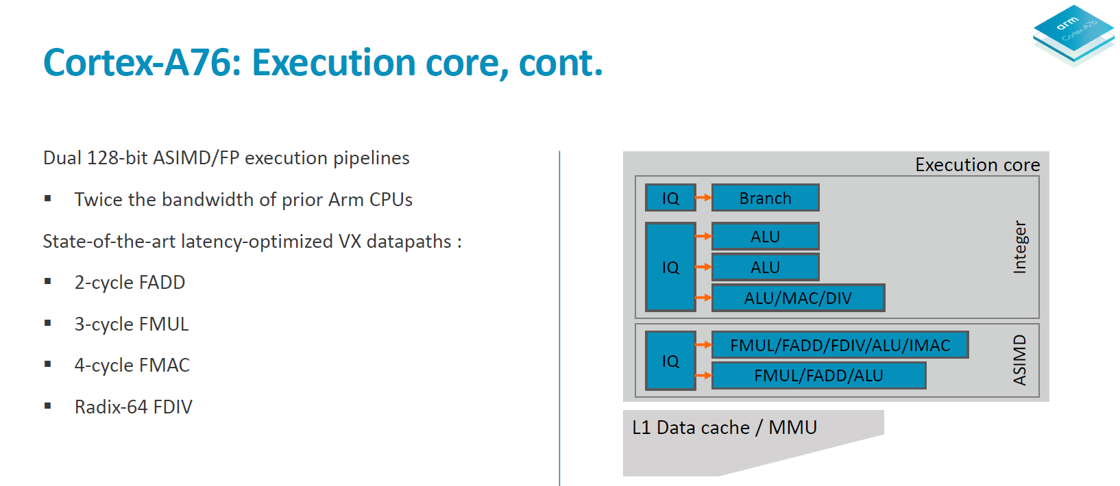
Two load/store units are the remaining ports of the integer core and are each served by two 12 deep issue queues. The issue queue stages are 3 cycles deep and while I mentioned that the rename/dispatch is 1 stage deep, the dispatch stage actually overlaps with the first cycle of the issue queues stages.
The ASIMD/floating point core contains two pipelines which are served by two 16-deep issue queues.
When it comes to the backend of a CPU core the two most important metrics are instruction throughput and latency. Where the A76 in particular improves a lot is in terms of instruction latency as it’s able to shave off cycles on very important instructions.
To better overview the improvements I created a table with the most common instruction types. The execution throughput and latencies presented here are for AArch64 instructions and if not otherwise noted represent operations on 64-bit data for integer and 64bit (double precision) FP.
| Backend Execution Throughput and Latency | ||||||
| Cortex-A75 | Cortex-A76 | Exynos-M3 | ||||
| Exec | Lat | Exec | Lat | Exec | Lat | |
| Integer Arithmetic (Add, sub) | 2 | 1 | 3 | 1 | 4 | 1 |
| Integer Multiply 32b | 1 | 3 | 1 | 2 | 2 | 3 |
| Integer Multiply 64b | 1 | 3 | 1 | 2 | 1 (2x 0.5) |
4 |
| Integer Multiply Accumulate | 1 | 3 | 1 | 2 | 1 | 3 |
| Integer Division 32b | 0.25 | 12 | 0.2 | < 12 | 1/12 - 1 | < 12 |
| Integer Division 64b | 0.25 | 12 | 0.2 | < 12 | 1/21 - 1 | < 21 |
| Move (Mov) | 2 | 1 | 3 | 1 | 3 | 1 |
| Shift ops (Lsl) | 2 | 1 | 3 | 1 | 3 | 1 |
| Load instructions | 2 | 4 | 2 | 4 | 2 | 4 |
| Store instructions | 2 | 1 | 2 | 1 | 1 | 1 |
| FP Arithmetic | 2 | 3 | 2 | 2 | 3 | 2 |
| FP Multiply | 2 | 3 | 2 | 3 | 3 | 4 |
| FP Multiply Accumulate | 2 | 5 | 2 | 4 | 3 | 4 |
| FP Division (S-form) | 0.2-0.33 | 6-10 | 0.66 | 7 | >0.16 (2x 1+/12) |
12 |
| FP Load | 2 | 5 | 2 | 5 | 2 | 5 |
| FP Store | 2 | 1-N | 2 | 2 | 2 | 1 |
| ASIMD Arithmetic | 2 | 3 | 2 | 2 | 3 | 1 |
| ASIMD Multiply | 1 | 4 | 1 | 4 | 1 | 3 |
| ASIMD Multiply Accumulate | 1 | 4 | 1 | 4 | 1 | 3 |
| ASIMD FP Arithmetic | 2 | 3 | 2 | 2 | 3 | 2 |
| ASIMD FP Multiply | 2 | 3 | 2 | 3 | 1 | 3 |
| ASIMD FP Chained MAC (VMLA) | 2 | 6 | 2 | 5 | 3 | 5 |
| ASIMD FP Fused MAC (VFMA) | 2 | 5 | 2 | 4 | 3 | 4 |
On the integer operations side the A76 improves the multiplication and multiply accumulate latencies from 3 cycles down to 2 cycles, with the throughput remaining the same when compared to the A75. Obviously because the A76 has 3 integer pipelines simple arithmetic operations see a 50% increase in throughput versus the A75’s 2 pipelines.
The much larger and important improvements can be found in the “VX” (vector execution) pipelines which are in charge of FP and ASIMD operations. Arm calls the new pipeline a “state-of-the-art” design and this is finally the result that’s been hyped up for several years now.
Floating point arithmetic operations have been reduced in latency from 3 cycles down to 2 cycles, and multiply accumulate has also shaved off a cycle from 5 cycles down to 4.
What Arm means by the “Dual 128bit ASIMD” with doubled execution bandwidth is that for the A75 and prior only one of the vector pipelines was capable of 128bit while the other one was still 64-bit. For the A76 both vector pipelines are 128-bit now so quad-precision operations see a doubling of the execution throughput.
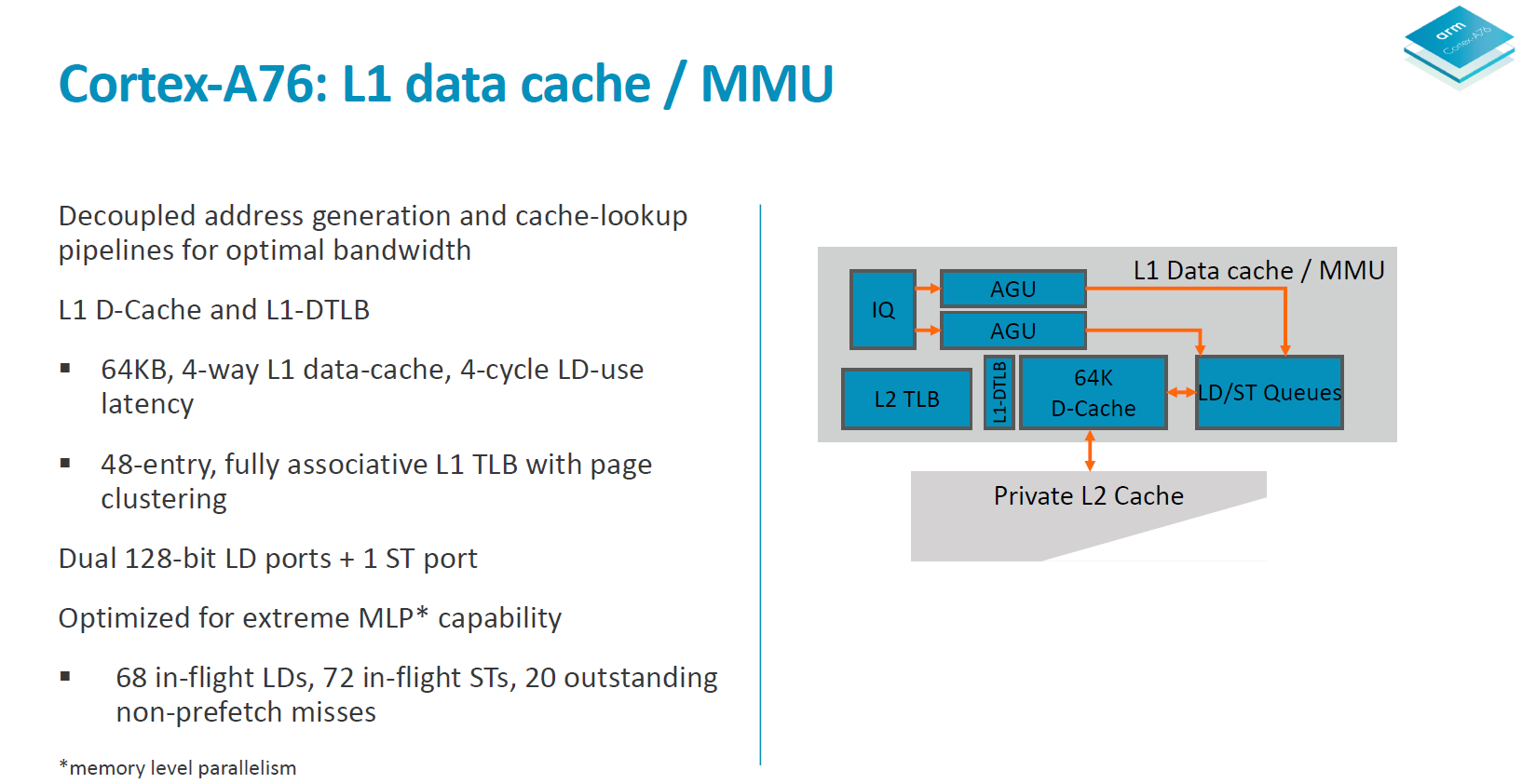
Moving onto more details of the data handling side, we see the again the two load/store pipelines which was something first implemented on the A73 and A75. Although depicted as one issue queue in the slide, the LD/S pipelines each have their own queues at 16 entries deep.
The data cache is fixed at 64KB and is 4-way associative. Load latency remains at 4 cycles. The DTLBs run a separate pipeline as tag and data lookup. Arm’s goals here is aiming for maximum MLP/ memory level parallelism to be able to feed the core.
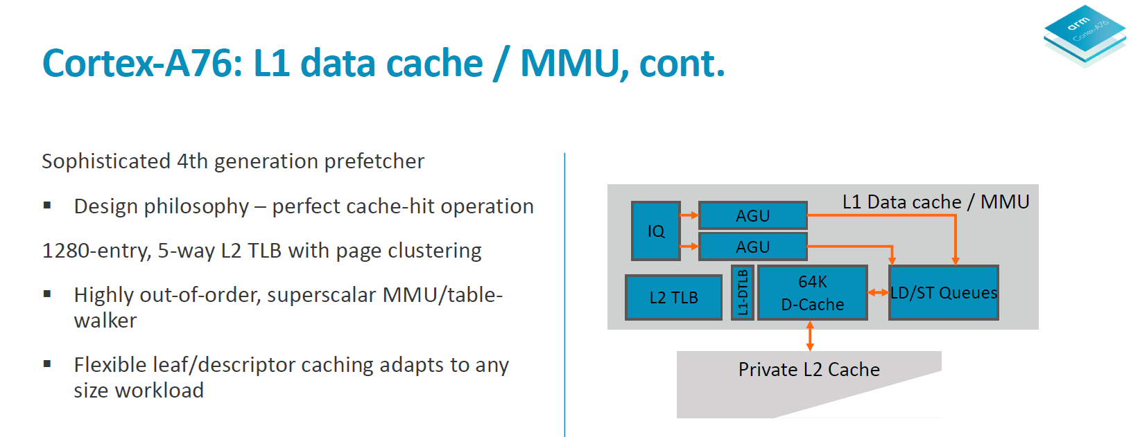
In a perfect machine everything would be already located in the caches, so it’s important to have very robust prefetching capabilities. On the A76 we see a new 4th generation prefetchers introduced to get nearer to this goal of perfect cache-hit operation. In all the A76 has 4 different prefetching engines running in parallel looking at various data patterns and loading data into the caches.
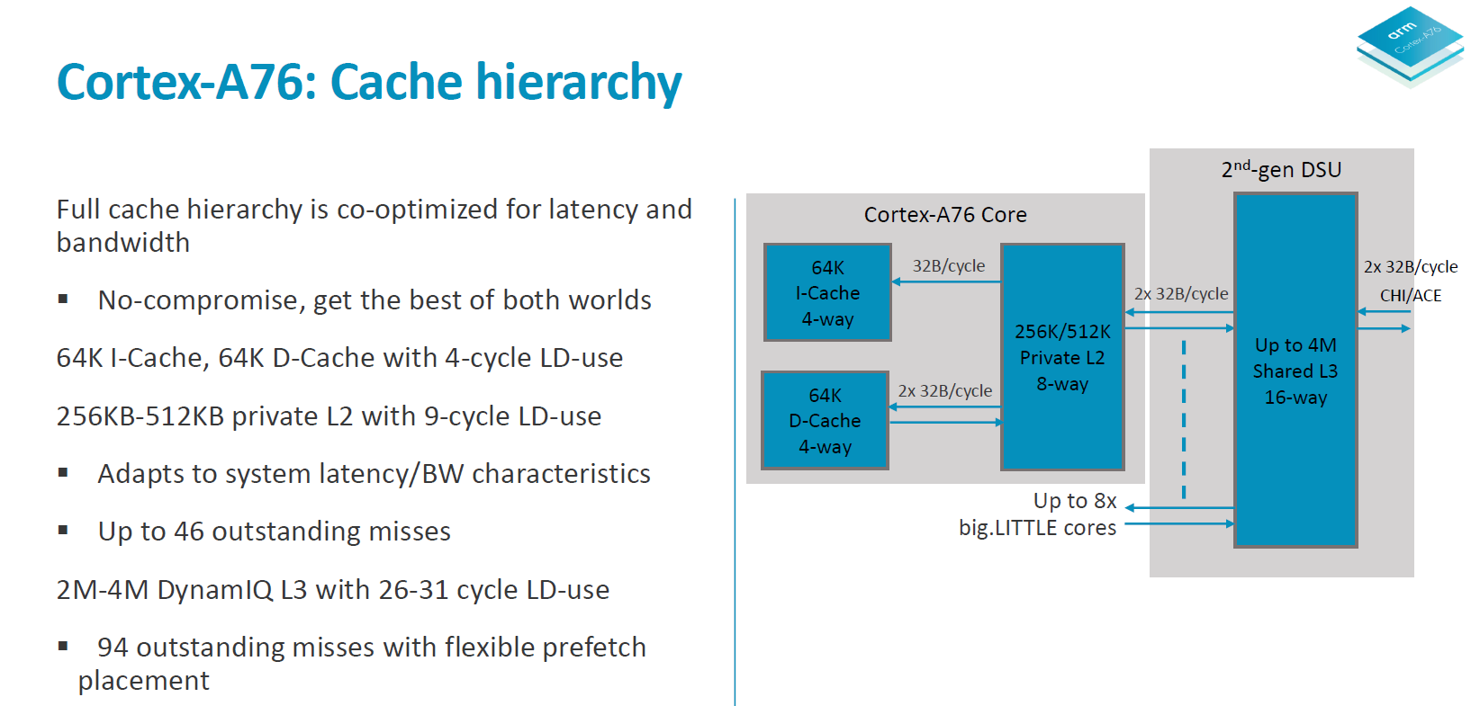
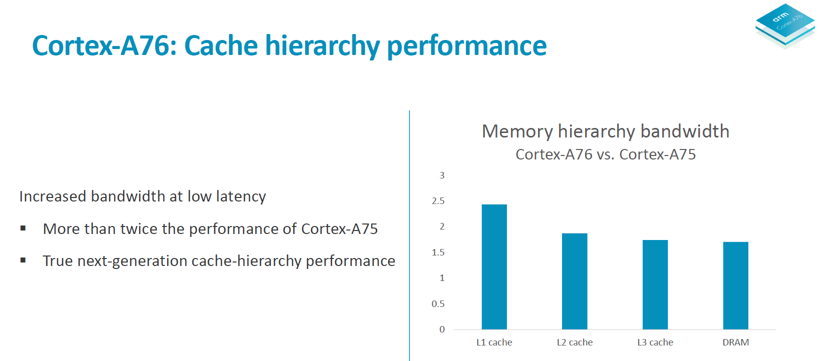
In terms of the A76 cache hierarchy Arm is said to have made no compromises and got the best of both worlds in terms of bandwidth and latency. The 64KB L1 instruction cache reads up to 32B/cycle and the same bandwidth applies to the L1 data cache in both directions. The L1 is a writeback cache. The L2 cache is configurable in 256 or 512KB sizes and is D-side inclusive with the same 2x 32B/cycle write and read interfaces up to the exclusive L3 cache in the 2nd generation DSU.
Overall the microarchitectural improvements on the core are said to improve memory bandwidth to DRAM by up to 90% in microbenchmarks.
All in all the microarchitecture of the A76 could be summed up in a few focus design points: Maximise memory performance throughout the core by looking at every single cycle. During the design phase the engineers were looking at feature changes with a sensitivity of up to 0.25% in performance or power – if that metric was fulfilled then it was deemed to be a worthwhile change in the core. Small percentages then in turn add up to create significant figures in the end product.
The focus on bandwidth on latency is said to have been extreme, and Arm was very adamant in re-iterating that to be able to take full advantage of the microarchitecture that vendors need to implement an equally capable memory subsystem on the SoC to see full advantages. A figure that was put out there was 0.25% of performance per nanosecond of latency to main memory. As we’ve seen in the Snapdragon 845 one of the reasons the SoC didn’t quite reach Arm’s projected performance metrics was the degraded memory latency figures which might have been introduced by the L4 system cache in the SoC. In the future vendors will need to focus more on providing latency sensitive memory subsystems as otherwise they’ll be letting free performance and power on the table with differences that could amount to basically a generational difference in CPU IP.


123 Comments
View All Comments
id4andrei - Thursday, May 31, 2018 - link
Apple has the manpower and funds to spend extensively for a huge chip for they are free to do things for their own glory. QCOMM designs chip for others to use and must design for price points. They must do so efficiently and maximize yields. ARM provides base designs that others can outright use or customize, you can't really blame ARM here. NVIDIA has no modem.syxbit - Thursday, May 31, 2018 - link
I get that, but you're missing the point. Sure, the budget phones have a strict budget.An $800 Android flagship should not be tight on the SoC budget. If QCOMM sold an ultra high snapdragon that could compete with the A12 you had better believe the Galaxy S10 and Pixel 3 phones would pay to use it.
truckasaurus - Thursday, May 31, 2018 - link
Apple has the convenience of designing to a very specific application. Qualcomm ultimately has to create something that can go into many platforms that are defined no more completely than 'high-end mobile'. That's like asking why the 3.5L V6 that's in most of Toyota's vehicles only makes 268 hp, but in the Lotus Evora 400, which uses the same engine, makes 400 hp. It's because it has been tweaked for a very specific application.serendip - Thursday, May 31, 2018 - link
Then they should sell supercharger kits for Qualcomm chips ;-)That is how the Evora V6 gets 400 hp compared to 280-300 hp on the latest non-turbo versions of that V6. The twin turbo version of that engine on the Lexus LS makes over 450 hp too.
truckasaurus - Thursday, May 31, 2018 - link
That's essentially what I'm getting at. Qualcomm makes the generic version of the engine that can go into a sedan, an SUV, a coupe, and a convertible and adequately power all of them. Apple says, we're only going to make 1 model of sports car and one large luxury sedan, and because we know exactly what our constraints are on these two platforms, we can add a turbo or a supercharger, we can tweak the timing, we can put a high-flow exhaust on it, etc.Pneumothorax - Friday, June 1, 2018 - link
Your point would make sense if the 845 were being used in low end Androids. Since it's pretty much only being used in high end designs, all out performance should've been the goal.syxbit - Thursday, May 31, 2018 - link
None of what you're saying makes sense. I simply think QCOMM and the rest are behind Apple because they can't do as good a job as Apple. It isn't because the market doesn't exist or because they need to build flexible designs.SirPerro - Friday, June 1, 2018 - link
Oh but many of us reading this conversation think all that really makes sense, and it really is because the market doesn't exist or because they need to build flexible designs.The car engine analogy was pretty great. It's exactly like that.
Threska - Thursday, May 31, 2018 - link
True. What Apple is good at is showing the potential for what's possible. Other's may have their reasons for not reaching it, but at least none can say it's not possible.shadowx360 - Thursday, May 31, 2018 - link
A lot of it comes down to power consumption. Samsung managed to get close to the A10 performance but at the cost of much higher power draw. With a 4 wide decoder instead of 6 wide, ARM is able to keep power usage in check and if their claims are to be believed, A10 performance at half the power is probably more desirable to the average consumer than A11/A12 performance at Snapdragon 810 levels of thermal throttle.