Arm's Cortex-A76 CPU Unveiled: Taking Aim at the Top for 7nm
by Andrei Frumusanu on May 31, 2018 3:01 PM EST- Posted in
- CPUs
- Arm
- Smartphones
- Mobile
- SoCs
- Cortex-A76
Cortex A76 µarch - Backend
Switching to the back-end of the core we have a look at the execution core.

The integer core contains 6 issue queues and execution ports (4 depicted in the slide plus 2 load/store pipelines). There are 3 integer execution pipelines – two ALUs capable of simple arithmetic operations and a complex pipeline handling also multiplication, division and CRC ops. The three integer pipelines are served by 16 deep issue queues. The same size issue queue can also be found serving the single branch execution port.
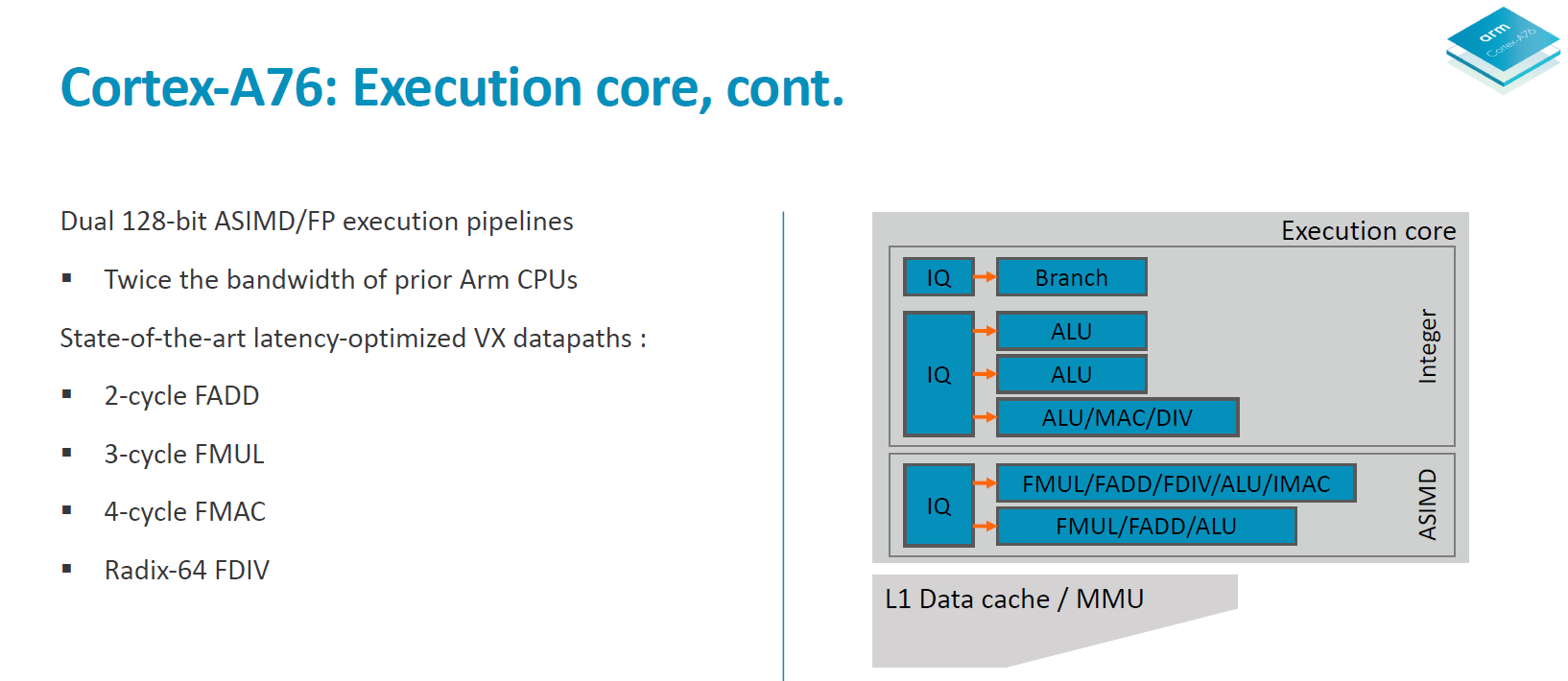
Two load/store units are the remaining ports of the integer core and are each served by two 12 deep issue queues. The issue queue stages are 3 cycles deep and while I mentioned that the rename/dispatch is 1 stage deep, the dispatch stage actually overlaps with the first cycle of the issue queues stages.
The ASIMD/floating point core contains two pipelines which are served by two 16-deep issue queues.
When it comes to the backend of a CPU core the two most important metrics are instruction throughput and latency. Where the A76 in particular improves a lot is in terms of instruction latency as it’s able to shave off cycles on very important instructions.
To better overview the improvements I created a table with the most common instruction types. The execution throughput and latencies presented here are for AArch64 instructions and if not otherwise noted represent operations on 64-bit data for integer and 64bit (double precision) FP.
| Backend Execution Throughput and Latency | ||||||
| Cortex-A75 | Cortex-A76 | Exynos-M3 | ||||
| Exec | Lat | Exec | Lat | Exec | Lat | |
| Integer Arithmetic (Add, sub) | 2 | 1 | 3 | 1 | 4 | 1 |
| Integer Multiply 32b | 1 | 3 | 1 | 2 | 2 | 3 |
| Integer Multiply 64b | 1 | 3 | 1 | 2 | 1 (2x 0.5) |
4 |
| Integer Multiply Accumulate | 1 | 3 | 1 | 2 | 1 | 3 |
| Integer Division 32b | 0.25 | 12 | 0.2 | < 12 | 1/12 - 1 | < 12 |
| Integer Division 64b | 0.25 | 12 | 0.2 | < 12 | 1/21 - 1 | < 21 |
| Move (Mov) | 2 | 1 | 3 | 1 | 3 | 1 |
| Shift ops (Lsl) | 2 | 1 | 3 | 1 | 3 | 1 |
| Load instructions | 2 | 4 | 2 | 4 | 2 | 4 |
| Store instructions | 2 | 1 | 2 | 1 | 1 | 1 |
| FP Arithmetic | 2 | 3 | 2 | 2 | 3 | 2 |
| FP Multiply | 2 | 3 | 2 | 3 | 3 | 4 |
| FP Multiply Accumulate | 2 | 5 | 2 | 4 | 3 | 4 |
| FP Division (S-form) | 0.2-0.33 | 6-10 | 0.66 | 7 | >0.16 (2x 1+/12) |
12 |
| FP Load | 2 | 5 | 2 | 5 | 2 | 5 |
| FP Store | 2 | 1-N | 2 | 2 | 2 | 1 |
| ASIMD Arithmetic | 2 | 3 | 2 | 2 | 3 | 1 |
| ASIMD Multiply | 1 | 4 | 1 | 4 | 1 | 3 |
| ASIMD Multiply Accumulate | 1 | 4 | 1 | 4 | 1 | 3 |
| ASIMD FP Arithmetic | 2 | 3 | 2 | 2 | 3 | 2 |
| ASIMD FP Multiply | 2 | 3 | 2 | 3 | 1 | 3 |
| ASIMD FP Chained MAC (VMLA) | 2 | 6 | 2 | 5 | 3 | 5 |
| ASIMD FP Fused MAC (VFMA) | 2 | 5 | 2 | 4 | 3 | 4 |
On the integer operations side the A76 improves the multiplication and multiply accumulate latencies from 3 cycles down to 2 cycles, with the throughput remaining the same when compared to the A75. Obviously because the A76 has 3 integer pipelines simple arithmetic operations see a 50% increase in throughput versus the A75’s 2 pipelines.
The much larger and important improvements can be found in the “VX” (vector execution) pipelines which are in charge of FP and ASIMD operations. Arm calls the new pipeline a “state-of-the-art” design and this is finally the result that’s been hyped up for several years now.
Floating point arithmetic operations have been reduced in latency from 3 cycles down to 2 cycles, and multiply accumulate has also shaved off a cycle from 5 cycles down to 4.
What Arm means by the “Dual 128bit ASIMD” with doubled execution bandwidth is that for the A75 and prior only one of the vector pipelines was capable of 128bit while the other one was still 64-bit. For the A76 both vector pipelines are 128-bit now so quad-precision operations see a doubling of the execution throughput.
Moving onto more details of the data handling side, we see the again the two load/store pipelines which was something first implemented on the A73 and A75. Although depicted as one issue queue in the slide, the LD/S pipelines each have their own queues at 16 entries deep.
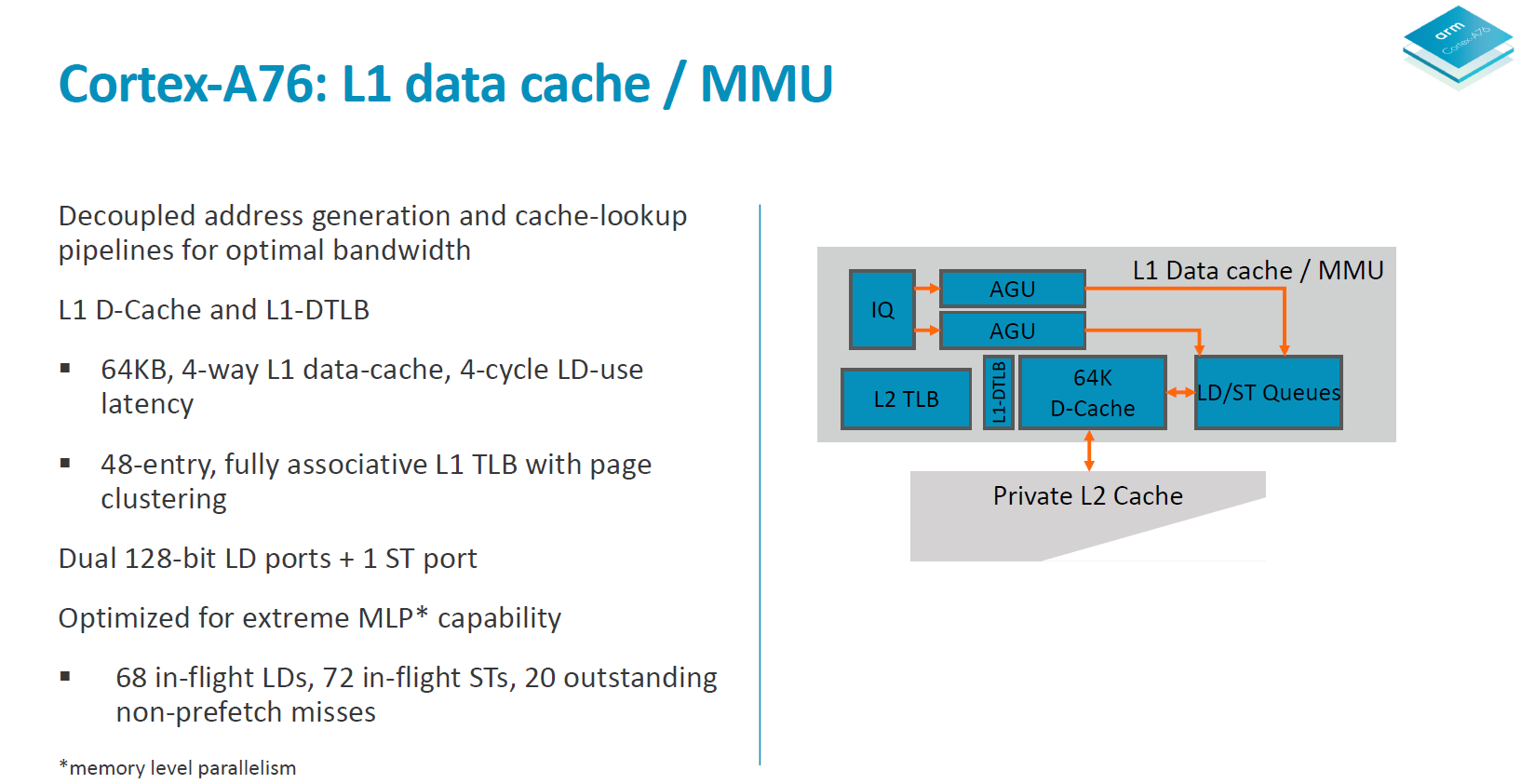
The data cache is fixed at 64KB and is 4-way associative. Load latency remains at 4 cycles. The DTLBs run a separate pipeline as tag and data lookup. Arm’s goals here is aiming for maximum MLP/ memory level parallelism to be able to feed the core.
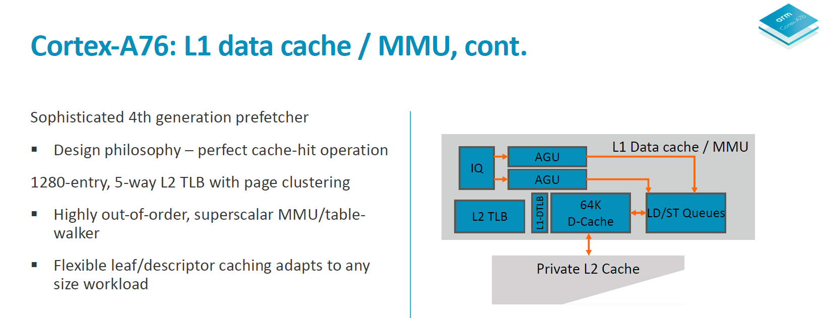
In a perfect machine everything would be already located in the caches, so it’s important to have very robust prefetching capabilities. On the A76 we see a new 4th generation prefetchers introduced to get nearer to this goal of perfect cache-hit operation. In all the A76 has 4 different prefetching engines running in parallel looking at various data patterns and loading data into the caches.
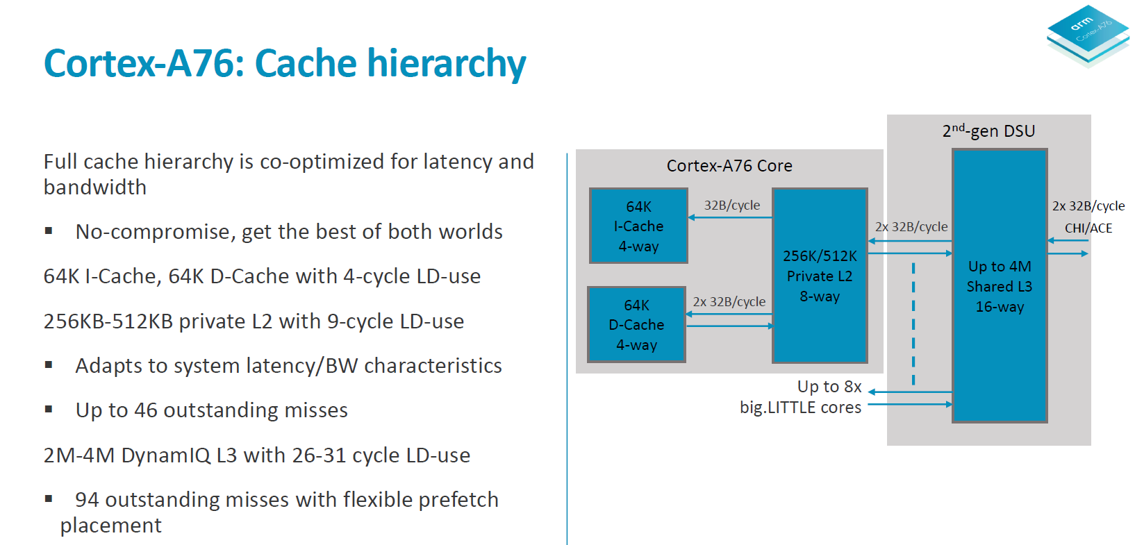
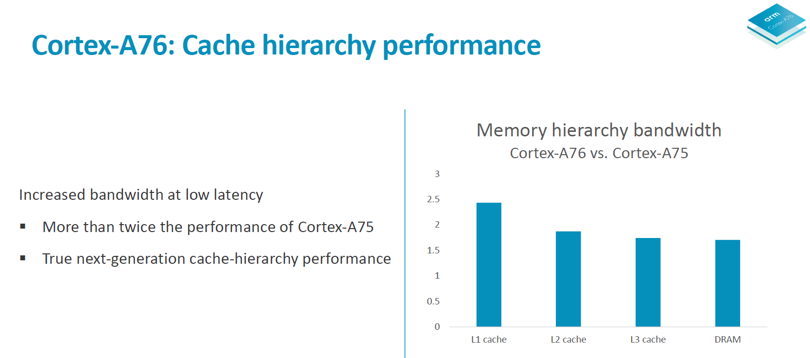
In terms of the A76 cache hierarchy Arm is said to have made no compromises and got the best of both worlds in terms of bandwidth and latency. The 64KB L1 instruction cache reads up to 32B/cycle and the same bandwidth applies to the L1 data cache in both directions. The L1 is a writeback cache. The L2 cache is configurable in 256 or 512KB sizes and is D-side inclusive with the same 2x 32B/cycle write and read interfaces up to the exclusive L3 cache in the 2nd generation DSU.
Overall the microarchitectural improvements on the core are said to improve memory bandwidth to DRAM by up to 90% in microbenchmarks.
All in all the microarchitecture of the A76 could be summed up in a few focus design points: Maximise memory performance throughout the core by looking at every single cycle. During the design phase the engineers were looking at feature changes with a sensitivity of up to 0.25% in performance or power – if that metric was fulfilled then it was deemed to be a worthwhile change in the core. Small percentages then in turn add up to create significant figures in the end product.
The focus on bandwidth on latency is said to have been extreme, and Arm was very adamant in re-iterating that to be able to take full advantage of the microarchitecture that vendors need to implement an equally capable memory subsystem on the SoC to see full advantages. A figure that was put out there was 0.25% of performance per nanosecond of latency to main memory. As we’ve seen in the Snapdragon 845 one of the reasons the SoC didn’t quite reach Arm’s projected performance metrics was the degraded memory latency figures which might have been introduced by the L4 system cache in the SoC. In the future vendors will need to focus more on providing latency sensitive memory subsystems as otherwise they’ll be letting free performance and power on the table with differences that could amount to basically a generational difference in CPU IP.


123 Comments
View All Comments
name99 - Friday, June 1, 2018 - link
FFS. the issue is NOT "Older batteries might not be able to supply enough power for a big core", it is that the battery cannot supply enough CURRENT.If you can't be bothered to understand the underlying engineering issue and why the difference between current and power matters, then your opinions on this issue are worthless.
serendip - Friday, June 1, 2018 - link
Whoa, chill there buddy, I'm not an electrical engineer.name99 - Friday, June 1, 2018 - link
"Does anyone actually use the full performance of the A11 or A12 in daily tasks? "Absolutely. I've updated iPhones every two years, and every update brings a substantial boost in "fluidity" and just general not having to wait. I can definitely feel the difference between my iPhone 7 and my friend's iPhone X; and I expect I will likewise feel the difference when I get my iPhone 2018 edition (whatever they are naming them this year...)
Now if you want to be a tool, you can argue "that's because Apple's software sux. Bloat, useless animations, last good version of iOS was version 4, blah blah". Whatever.
MOST people find more functionality distributed throughout the dozens of little changes of each new version of the OS, and MOST people find the "texture" of the OS (colors, animations, etc) more pleasant than having some sort of text only Apple II UI, though doubtless that could run at a 10,000 fps.
So point is, yeah, you DO notice the difference on phones. Likewise on iPads. I use my iPad to read technical PDFs, and again, each two year update provides a REALLY obvious jump in how quickly complicated PDF pages render. With my very first iPad 1 there was a noticeable wait almost every page (only hidden, usually, because of page caching). By the A10X iPad Pro it's rare to encounter a PDF page that ever makes you wait, cached or not.
I've also talked about in the past about Wolfram Player, a subset of Mathematica for iPad. This allows you to interact with Mathematica "animations" (actually they're 3D interactive objects you construct that change what is displayed depending on how you move sliders or otherwise tweak parameters). These are calculating what's to be displayed (which might be something like numerically solving a partial differential equation, then displaying the result as a 3D object) in realtime as you move a slider.
Now this is (for now) pretty specialized stuff. But Wolfram's goal, as they fix the various bugs in the app and implement the bits of Mathematica that don't yet work well (or at all), is for these things to be the equivalent of video today. We used to put up with explanations (in books, or newspapers) that were just words. Then we got BW diagrams. Then we got color diagrams. Then we got video. Now we have web sites like NYT and Vox putting up dynamic explainers where you can move sliders --- BUT they are limited to the (slow) performance of browsers, and are a pain to construct (both the UI, and the underlying mathematical simulation). Something like Mathematica's animations are vastly more powerful, and vastly easier to create. One day these will be as ubiquitous as video is today, just one more datatype that gets passed around. But for them to work well requires a CPU that can numerically solve PDEs in real time on your mobile device...
techconc - Tuesday, June 5, 2018 - link
The benefits of having a fast single core are seen on most common operations, including UI and scrolling, etc. Moreover, Apple has demonstrated that a powerful core can in fact be more efficient in race to sleep conditions whereby it completes the work more quickly then sleeps. The overall effect is a more responsive system that is just as efficient overall.tipoo - Tuesday, September 4, 2018 - link
Sure, every time I render a webpage.ZolaIII - Friday, June 1, 2018 - link
Well let's put it this way the A73 which is two instructions wide had a no problems on 14 nm FinFET, A76 is 4 instruction wide & for a sakes of argument let's say 2x the size. So switching from 14 nm to 7nm (60% reduction on power) cower it, A76 is approximately 65% faster than A73 MHz per MHz so its able to deliver approximately the 1.8x performance per same DTP. Second part is a manufacturing process in comparison to the core size. The FinFET structure transistors leak as hell when the 2.1~2.2 GHz limit is reached disregarding of OEM, vendor/foundry. So if you employ 50% wider core's (6 instructions wide) that won't cross the 2.1~2.2 GHz limit it's not the same as if you push the limit of the 4 instructions wide one to 3GHz as the power consumption will be doubled compared to the same one operating on 2.1~2.2 GHz & in the end you lose both on theoretical true output (performance) and power consumption metric but it still costs you 33% less. In reality it's much harder to feed optimally the wider core (especially on something which is mobile OS). ARM (cowboy camp) did a great work optimising instruction latency and cache latency/true output which will both increase real instruction output per clock & help predictor without significant increase in needed resources (cost - size) & A76 is a first of it's kind (CPU ever) regarding implanted solution for this. However thing that ARM didn't deliver is a better primary work horse which could make a difference in base user experience. A55 aren't exactly the power haus regarding performance & now their is more headroom regarding power when scaled down to the 7 nm, enough for let's say A73 on slightly lower clocks to replace the A55 (A73 is 1.6x integer performance of A55 MHz/MHz so A73 @ 1.7GHz = A55 @ 2.7 GHz while switching from 14 to 7nm would make DTP of A55 to A73 the same). But A73 doesn't work on DinamIQ cluster. So there is a need for the new two instructions wide OoO core with merged architectural advancements (front end, predictor, cache, ASIMD...) as in order ones did hit the brick wall long time ago.vladx - Friday, June 1, 2018 - link
> So switching from 14 nm to 7nm (60% reduction on power)That might've been true if both 14nm and 7nm fab processes were actually the real deal. But alas, they are not.
ZolaIII - Saturday, June 2, 2018 - link
Based on the TSMC projections 60% power reduction.beginner99 - Monday, June 4, 2018 - link
The things is that CPU power use might already be a small part of phone power use. The display usually being the main consumer and when the display isn't running, most likely the big core will also not be running. Saving 40% power sounds great on paper. But in real designs it will already be smaller and the total impact on phone battery life will be much, much smaller. Single-digit percentage probably depending on how much you use. The more it is idle, the less the big core efficiency matters.Dazedconfused - Thursday, May 31, 2018 - link
I get this, but when comparing an iPhone x and say an Android flagship next to each other in pretty much every day to day task, they appear evenly matched. There are some good comparisons on YouTube. There are definitely strengths to each platform, but it's not clear cut at all