Intel's Architecture Day 2018: The Future of Core, Intel GPUs, 10nm, and Hybrid x86
by Dr. Ian Cutress on December 12, 2018 9:00 AM EST- Posted in
- CPUs
- Memory
- Intel
- GPUs
- DRAM
- Architecture
- Microarchitecture
- Xe
Ice Lake 10nm Xeon Scalable On Display
One of the more sedate talks at the event was discussing Intel’s approach in the datacenter. We’ve covered this story in detail, especially at Intel’s Data-Centric Summit only a few months ago. Intel has stated that Cascade Lake and Cooper Lake are the next two products for the enterprise market, both built on 14nm, focusing on enhanced security as well as AI instructions to help with acceleration. We also know that after these two Intel will have Ice Lake Scalable built on 10nm, but that’s about it.
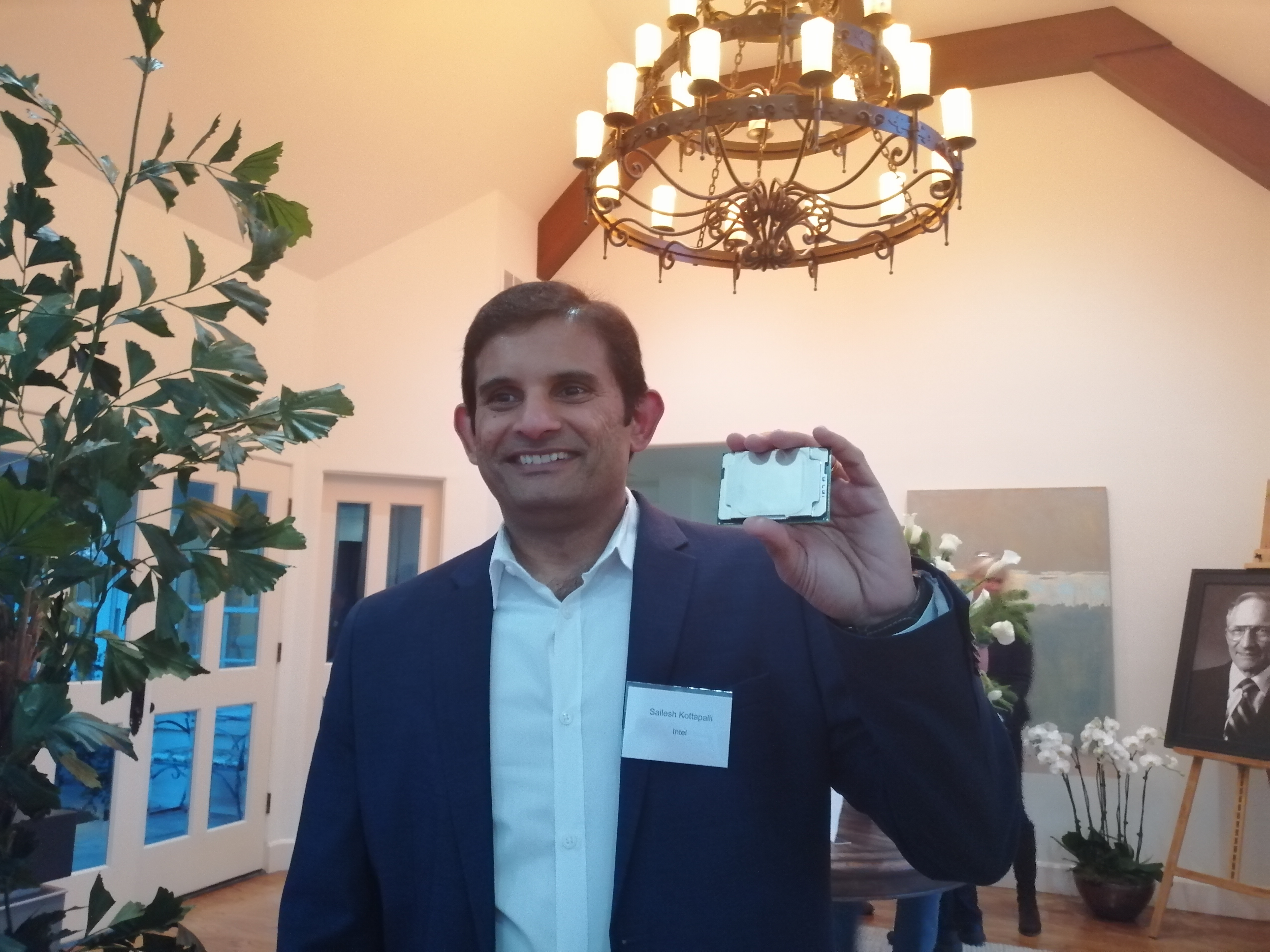
To be honest, we don’t actually know much more than what we did back then. Intel confirmed that Ice Lake will be built using Sunny Cove cores. But Intel also showed off what they said was an Ice Lake Xeon 10nm processor and package, as shown in the image above.
Color me skeptical, but what was held up is likely either not ICL-SP or just silicon that doesn’t work. In order to make those products, Intel would have to have pumped out at least one large (350mm2+?) die that worked and then put it into a package with a heatspreader. Intel finally seems to be happy discussing a few products on 10nm, as shown at this event, but all the 10nm hardware is based on tiny 100mm2 or smaller silicon. Given Intel’s documented problems, I would have loved that CPU that was held up in the air to be Ice Lake-SP. But I’ll need to see something more concrete to believe it at this point; it’s too much of a jump.
Ending Intel’s Architecture Day
As I’m writing this, it is 3am PT and only a couple of hours away from Intel’s listed embargo time. The event finished 10 hours ago (a few of us skipped the end event drinks to get to writing) and despite the short time to write it all up, it was a good event overall. For the first time in a good while, Intel decided to talk shop, and in an honest way with very little hand waving. One could argue that in every discussion point, Intel raised more questions than they answered, but the positive here is that questions are being answered, and Intel is willing to share things like roadmaps into 2021, demonstrations of some exciting new products for 2019/2020, and a taste of how they are progressing in both manufacturing and microarchitecture. Hopefully Intel will feel the same and this can become a yearly cadence. The trio of Keller, Koduri, and Murthy, is a strong team to field to the press, and this event fits that bill.
To end this piece, I’m going to put in the Q&A section from day’s presentations, as well as some of the questions put in my particular round-table. It’s an interesting read, and it helps that Jim is full of memorable quotes.


148 Comments
View All Comments
f1nalpr1m3 - Wednesday, December 12, 2018 - link
Yeah, they totally put it together in three weeks and everything.Get a clue.
pkgtech - Thursday, December 20, 2018 - link
For years Sohail Ahmed was the roadblock to Intel doing any creative package technology by blocking silicon support. He finally was shown for what he was after 2+ year process technology delays and re-invented this. Good riddance SohailAdonisds - Wednesday, December 12, 2018 - link
How do the Intel process delays influence their microarchitecture plans? 10 nm was already supposed to be here and with it its new microarchitecture, Ice Lake. Does the Ice Lake design continue to get improved as the delays kept happening or was it finalized years ago? Why? What about the microarchutectures succeeding Ice Lake?III-V - Wednesday, December 12, 2018 - link
This is Ice Lake. Might be a 14nm port (unclear at this point why the name change), but it's at the very least a close relative.III-V - Wednesday, December 12, 2018 - link
Actually, given the name on the heat sink, it is probably just straight up Ice LakeHStewart - Thursday, December 13, 2018 - link
I believe the road map states Ice Lake will be on 10nm. More importantly it will be on Sunny Cove which is significant update to Architexture.AdhesiveTeflon - Wednesday, December 12, 2018 - link
Intel and their naming scheme....they should call one "blue slushie lake"prisonerX - Wednesday, December 12, 2018 - link
Plans? Intel are in full scale panic mode right now. I'm sure they have new plans every week.jjj - Wednesday, December 12, 2018 - link
LOL you went in full fanboy mode with the 144mm package being small.The package is that size for PoP, the die is much much smaller, they can fit way more 10nm cores than that in such a large area, even without a base die.
Anyway, there are no relevant details on Foveros and that's problematic. The first question is cost, then you would want to know details about pitch and so on. Intel is by no means the first to announce such a solution so the details are what matters.
This is how you get to a 3D monolithic die in some years so any foundry that wants to stay in the most advanced node game, needs to push the packaging roadmap.
Ian Cutress - Wednesday, December 12, 2018 - link
I specifically said the package was small, and the die was smaller than the package.