Intel's Architecture Day 2018: The Future of Core, Intel GPUs, 10nm, and Hybrid x86
by Dr. Ian Cutress on December 12, 2018 9:00 AM EST- Posted in
- CPUs
- Memory
- Intel
- GPUs
- DRAM
- Architecture
- Microarchitecture
- Xe
Intel’s First Fovoros and First Hybrid x86 CPU: Core plus Atom in 7 W on 10 nm
Perhaps someone will correct me, but I can’t ever remember a time when Intel has put multiple x86 cores of different configurations on the same bit of silicon (ed: Intel Edison). Ever since Arm starting doing it with its big.Little designs in smartphones, a perennial question was if Intel was going to do something similar, either with big and small Atom cores, or by moving a high-performance Core into the mix. When Intel left the smartphone and tablet market, we assumed the idea was dead. But, like a reanimated zombie, it has risen from the grave. Enter Intel’s Hybrid x86 CPU.
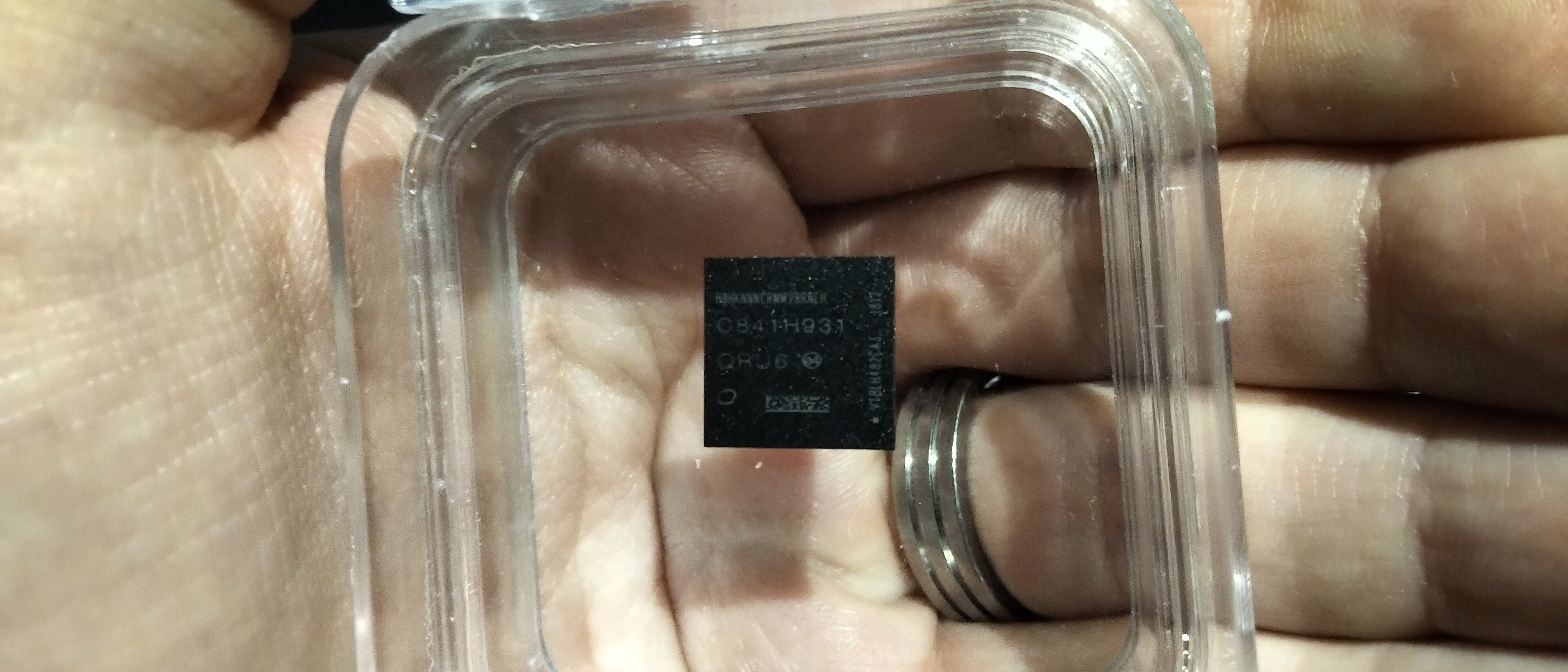
This tiny 12x12 package is built using Intel’s Fovoros technology, using a 22FFL IO chip as the active interposer connected with TSVs to a 10nm die that contains both a single Sunny Cove core and four Atom (Tremont?) cores. This tiny chip is smaller than a dime, and is designed to have a 2 mW standby power. It would appear that this chip is destined for mobile devices.
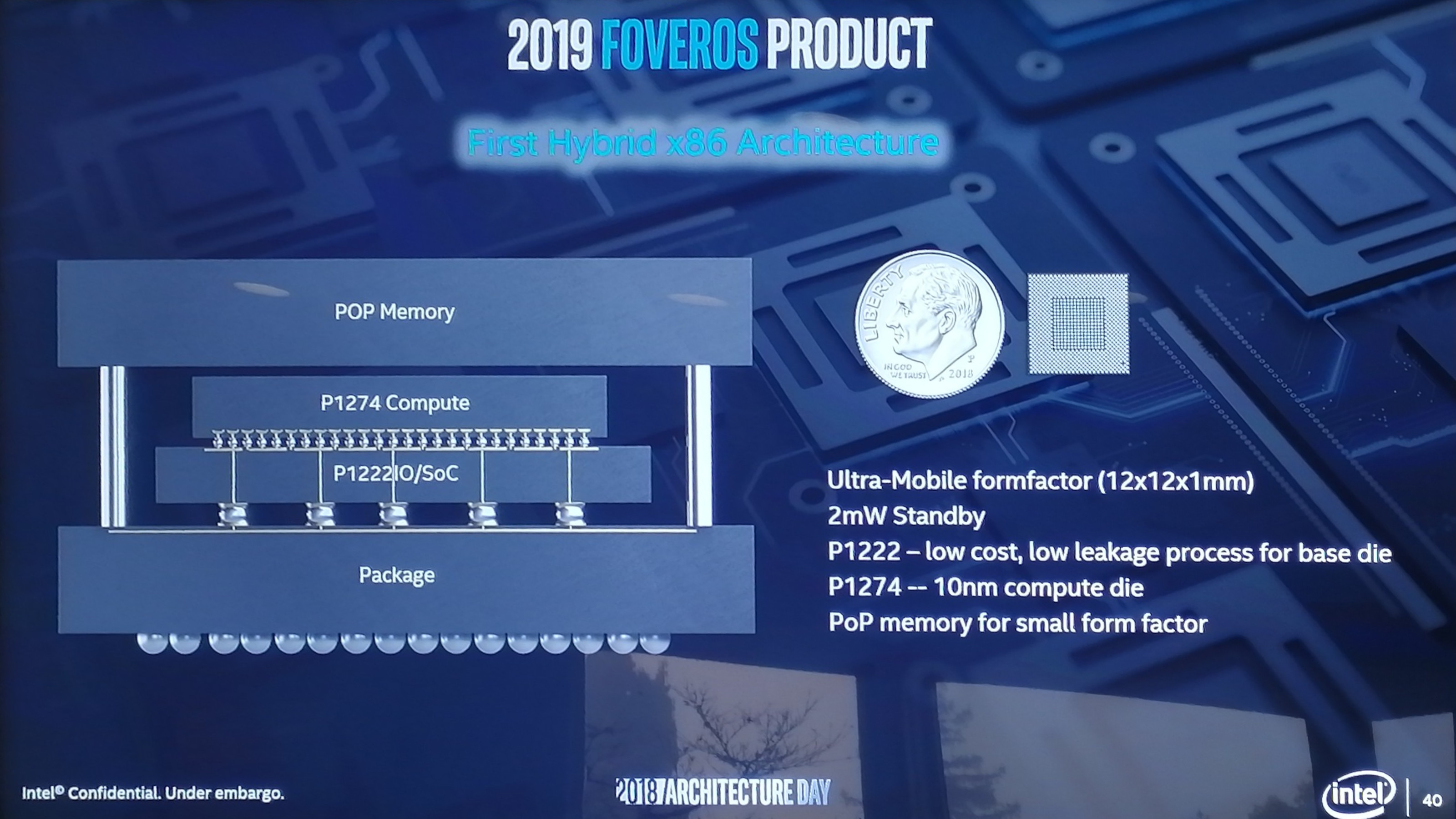
Here’s the manufacturing diagram, showing the idea that POP memory is placed over the Fovoros design to give the final product. Very much like a mobile chip.
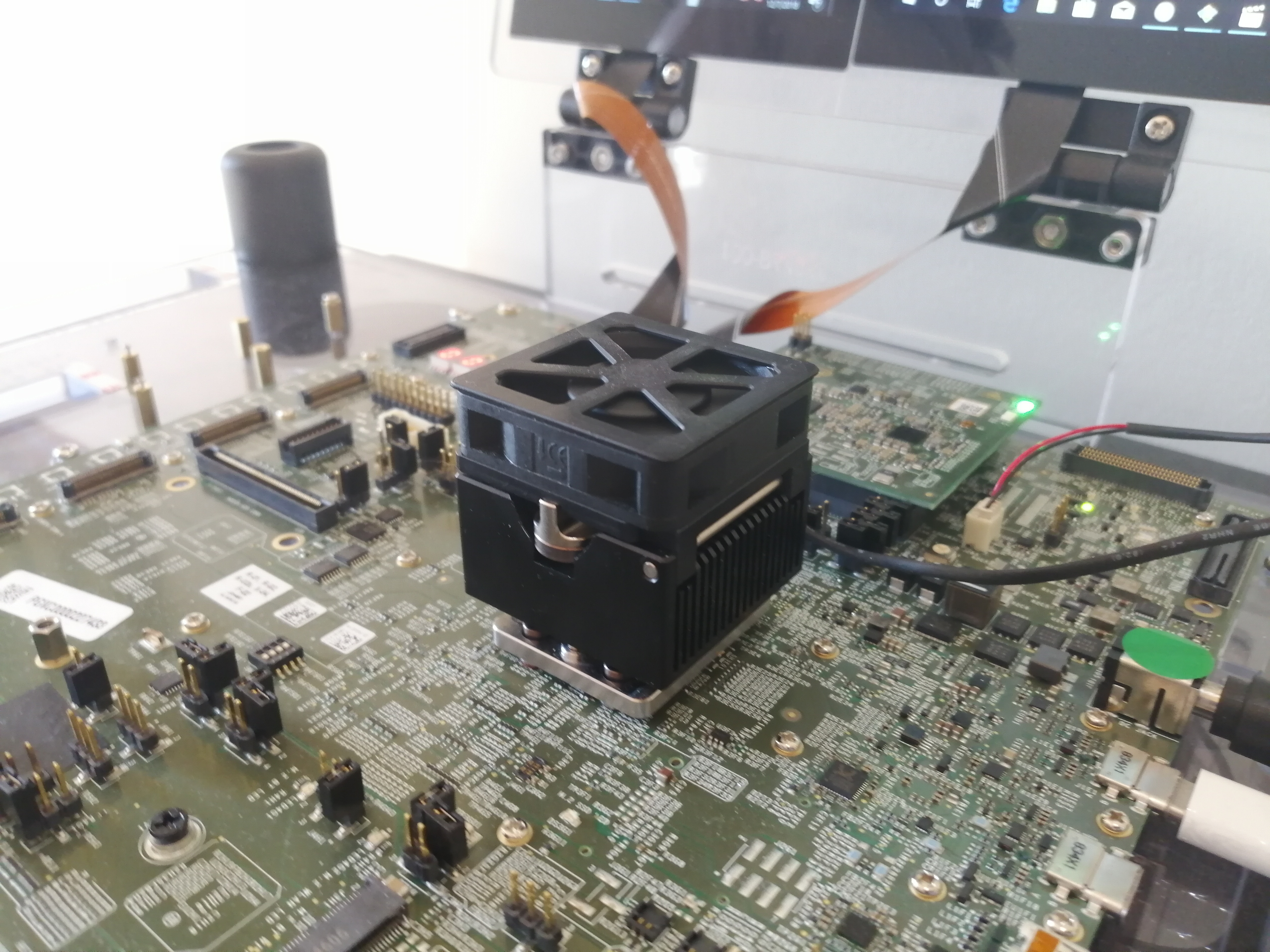
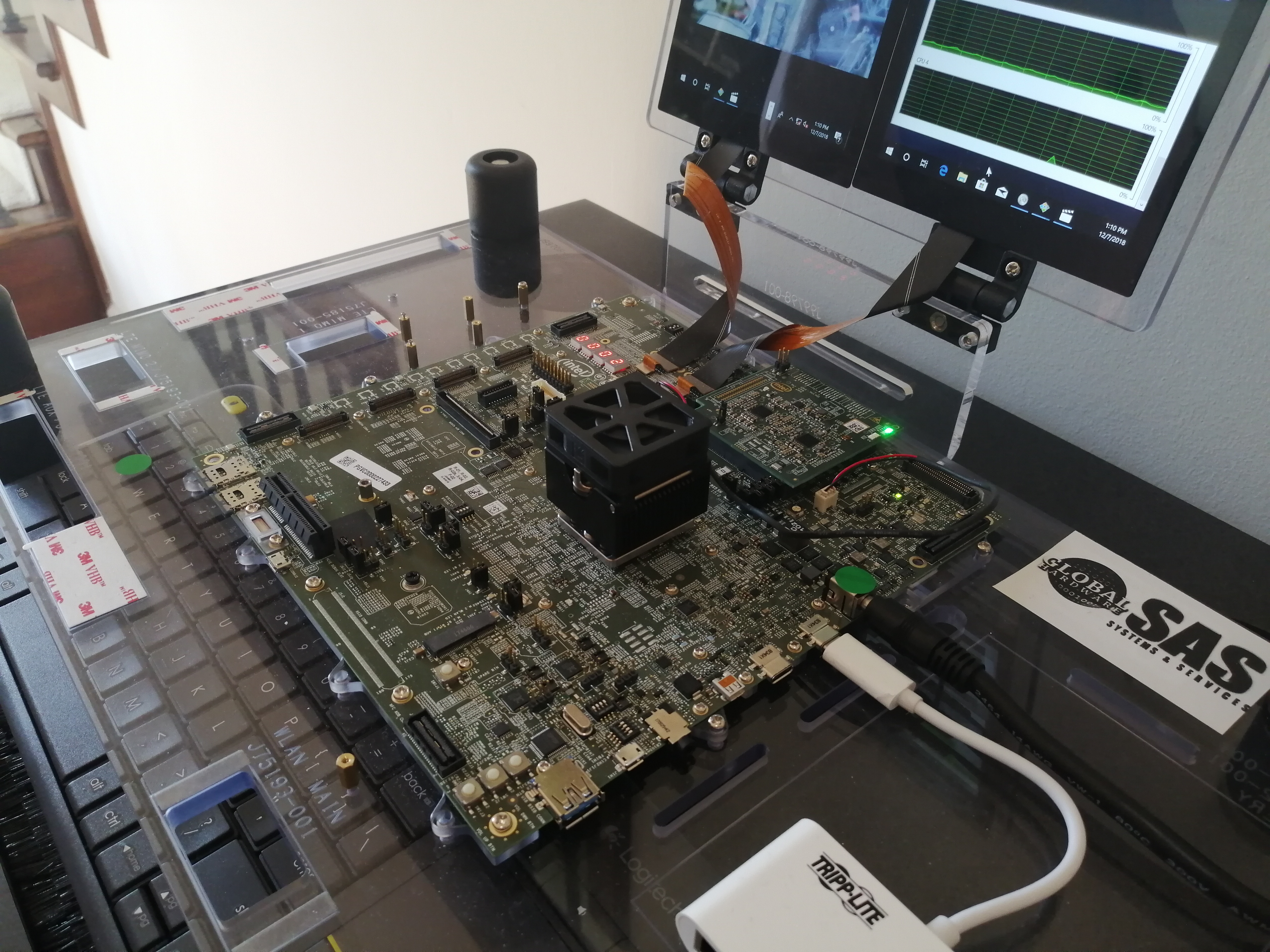
The demo system that Intel had on display looked similar to the previous Sunny Cove design, however this heatsink was smaller and it had a few different connectors. We were told that this chip will support PCIe for M.2 as well as UFS, both of which are found in mobile. There also looked like a couple of SIM card connectors on this motherboard.
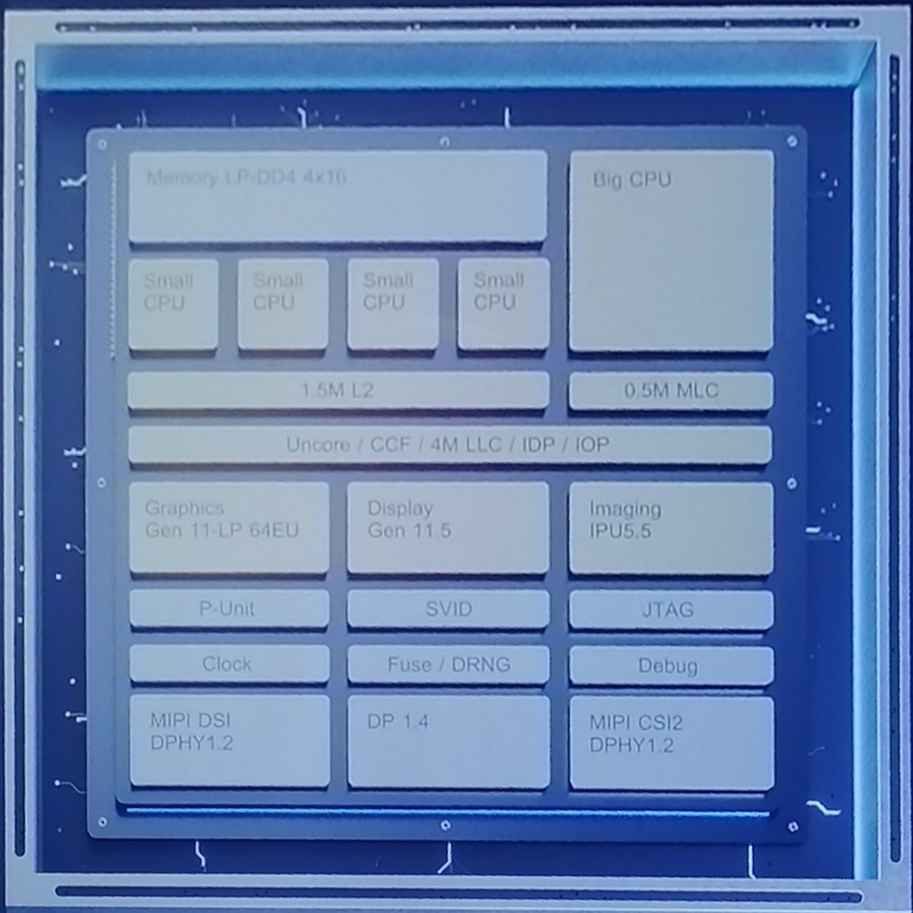
The key part of this discussion however is this block diagram that was on one of the Intel slides. Here we see a single ‘Big CPU’ with 0.5 MB of private medium level cache, four ‘Small CPU’s with a shared 1.5 MB L2 cache, an uncore that has 4MB of last level cache, a quad-channel memory controller (4x16-bit) with support for LPDDR4, a 64 EU design with Gen11 graphics, the Gen 11.5 display controller, a new IPU, MIPI support with DisplayPort 1.4, and all of this in a tiny package.
Seriously though, this has the potential to be a large revenue stream for Intel. They’ve made this chip, which allows the cores to enter C6 sleep states when not in use, that has a die size smaller than 12x12mm (144 mm2), and target the sub-7W fanless device market. That’s with a big Core, four Atom cores, and a GT2 64 EU design.
Intel actually says that the reason why this product came about is because a customer asked for a product of about this performance but with a 2 mW standby power state. In order to do this, Intel created and enhanced a number of technologies inside the company. The final product is apparently ideal for the customer, however the chip will also be made available for other OEMs.
In our Q&A session with the senior members of Intel, it was clear that this technology is still in its infancy, and Intel now has a new toy to play with. Jim Keller stated that internally they are trying lots of new things with this technology to see what works and what would make a good product, so we should be seeing more Foveros designs through 2019 and 2020.


148 Comments
View All Comments
jjj - Wednesday, December 12, 2018 - link
And you acted like someone clueless that has put all his savings in Intel's stock based on brad, "Large revenue stream" LOL, you don't know anything about the product, the target market, about the packaging solution but you get all wet.Anyway, took a look at the slides and they do actually provide some relevant details that yuo seem to not notice. They say face-face, bump pitch at 36um and bump density at 828.mm2.
Spunjji - Thursday, December 13, 2018 - link
Your comments are unnecessarily aggressive, dripping with unwarranted confidence and really unpleasant to read. Please spend more time offline.jjj - Wednesday, December 12, 2018 - link
For the hell of it, I'll add this IMEC slide (different versions out there but this one was the first i could find)http://www.techdesignforums.com/practice/files/201...
iwod - Thursday, December 13, 2018 - link
ignore the trolls.Raqia - Wednesday, December 12, 2018 - link
That's a nice fan on their fanless SoC design. It seems like Intel is really playing catch up with their ultra mobile designs (with a power envelope that's likely still above phones) fabbed on a late 10nm design and only now doing things like heterogeneous cores and PoP memory that the AX and Snapdragons have been doing for a few years now.I wonder what portion of that block diagram's compute reside on the P1222 (which looks bigger die space wise on their diagram than the P1274 but may pack fewer transistors.) They mentioned IO but it wouldn't make too much performance sense for caches and coherency to segregate the Big/Little cores onto separate dies, so it likely contains the ISPs and memory controllers. Where the GPU is located is another interesting question and no LTE modem can be seen on the block diagram. This is also likely to have higher packaging cost and worse integration than the AX, Kirins, PXX's or Snapdragons.
A5 - Wednesday, December 12, 2018 - link
Dev boards have fans because they don't have a chassis to sink heat into. If it's like every other dev board I've used, it is probably a 8k RPM screamer, too.The_Assimilator - Wednesday, December 12, 2018 - link
Seems like you failed to read page 4: "These were development systems with these funky looking heatsinks and loud fans to ensure there was no thermal throttling."Raqia - Wednesday, December 12, 2018 - link
My comment was in reference to their new Atom lineup which are supposed to be fanless, not Sunny Cove which operates in a much higher power envelope. Surely they could use a larger passive cooling unit to demonstrate what's supposed to be a key feature of that product; my other point is that Intel's aiming for something later next year that seems much less advanced than what Apple, Huawei, Mediatek, and Qualcomm already have in production today.The_Assimilator - Thursday, December 13, 2018 - link
And, again, the Fovoros setup was a demo board in the open air, not a production chip inside a device designed around dissipating the heat it outputs.Spunjji - Thursday, December 13, 2018 - link
If that's what you took from that part of the presentation then I feel you missed the point. What Intel are doing in terms of chip layout is something none of the companies you mentioned are able to do yet, which is the fundamental point here - whether it results in a useful product is another matter entirely, but it's still fascinating and not same-same.To back up the other people who responded to you, again, the fan is irrelevant. It's a dev board.