Intel Cascade Lake Xeon W-3200 Launched: Server Socket, 64 PCIe 3.0 lanes
by Dr. Ian Cutress on June 10, 2019 8:00 AM EST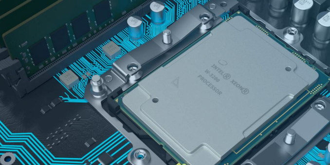
One of the quiet announcements that came out of Apple’s new Mac Pro announcement was the launch of Intel’s next generation Xeon W processors. Aside from being completely under the radar from a formal announcement, the new line of workstation focused CPUs heralds a few quirks: they are Cascade Lake based, they are only in the LGA3647 socket, and they have 64 available PCIe 3.0 lanes.
The current Xeon W product line, based on Skylake-SP, uses the common high-end desktop socket LGA2066, but with a workstation focused chipset. These processors are available up to eighteen cores, using Intel’s HCC 18-core die as the highest it will go. The other features of these processors include quad channel memory, 512GB ECC support, and up to 48 PCIe 3.0 lanes. What Intel has done for the next generation has bump it up to the server socket, which affords more memory channels, higher TDPs, more memory supported, and a higher core count.
The new Cascade Lake-based Xeon W-3200 family will be offered up to 28 cores, using Intel’s XCC 28-core die as the base for the high-end models. As a Cascade Lake processor, the new Xeon W will come with additional in-hardware fixes for some of the Spectre and Meltdown vulnerabilities, similar to the Cascade Lake Xeon Scalable Processors. Intel has also made a substantial change in the way that it intends to market its Xeon W processors, as the new models also change socket compared to the previous generation.
Historically we are afforded multiple generations of workstation CPU on the same socket, however at this time Intel has decided to forgo this application and move Xeon W from the LGA2066 socket to the LGA3647 socket, limiting users who wish to upgrade from their Xeon W-2100 processors. The new socket, combined with the new silicon, means that Intel can offer new Xeon W owners more features, although much to the chagrin of previous Xeon W owners. This doesn't exclude Intel launching another set of CPUs on the LGA2066 socket for upgrades, however given the lack of fanfare for this launch, it wouldn't seem likely that Intel has plans to do so.
The LGA3647 socket has been used in Xeon Scalable processors since Skylake-SP launch, and affords six full DDR4 memory channels. The silicon inside the new Xeon W does have six memory controllers, allowing it to take full use of this feature. (Technically the previous generation also had six memory controllers in the silicon, but the platform was limited to four, as per Intel’s product positioning strategy.)
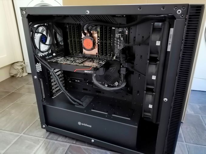
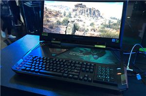
The LGA3647 system Intel sent with the last Xeon W Review Unit
As with the previous Xeon W, the cores are arranged in a block, and inside is a ‘Mesh’ which we’ve described in detail in previous reviews. One of the additional features for the Xeon W-3200 is the upgrade to a full 64 PCIe 3.0 lanes available for PCIe slots, up from the previous 48. This also makes Intel’s new Cascade Lake W-3200 family the x86 product that Intel offers with the most PCIe lanes.
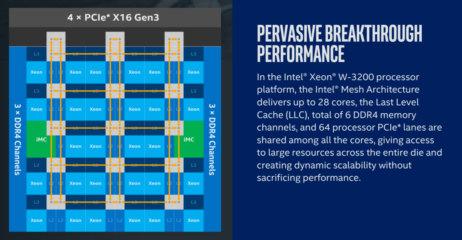
This is a bit of a technicality – previous Xeon SP and Xeon W did actually have 64 lanes on the silicon, however 16 of them were reserved for on-package chips, such as OmniPath. What Intel has done here is re-route them through the socket pins instead, allowing motherboard manufacturers to design a full x16/x16/x16/x16 layout or variants therein. This also means that the LGA3647 socket already had pins ready to be allocated to these PCIe lanes, so it would not have surprised me if Intel has already sold 64 PCIe lane custom versions to customers since the original Skylake-SP launch.

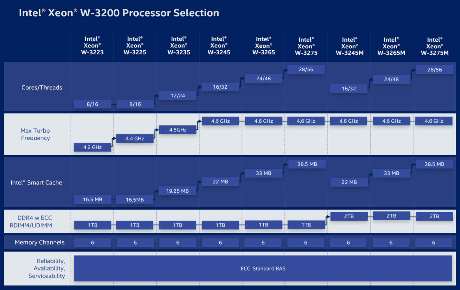
Here are the nine new CPUs:
| Intel Cascade Lake Xeon W-3200 Family | |||||||
| AnandTech | Cores Threads |
TDP | Base Freq |
Turbo 2.0 |
Turbo 3.0 |
DRAM | Price |
| W-3275M | 28C / 56T | 205 W | 2.5 GHz | 4.4 GHz | 4.6 GHz | 2 TiB | $7453 |
| W-3275 | 28C / 56T | 205 W | 2.5 GHz | 4.4 GHz | 4.6 GHz | 1 TiB | $4449 |
| W-3265M | 24C / 48T | 205 W | 2.7 GHz | 4.4 GHz | 4.6 GHz | 2 TiB | $6353 |
| W-3265 | 24C / 48T | 205 W | 2.7 GHz | 4.4 GHz | 4.6 GHz | 1 TiB | $3349 |
| W-3245M | 16C / 32T | 205 W | 3.2 GHz | 4.4 GHz | 4.6 GHz | 2 TiB | $5002 |
| W-3245 | 16C / 32T | 205 W | 3.2 GHz | 4.4 GHz | 4.6 GHz | 1 TiB | $1999 |
| W-3235 | 12C / 24T | 180 W | 3.3 GHz | 4.4 GHz | 4.5 GHz | 1 TiB | $1398 |
| W-3225 | 8C / 16T | 160 W | 3.7 GHz | 4.3 GHz | 4.4 GHz | 1 TiB | $1199 |
| W-3223 | 8C / 16T | 160 W | 3.5 GHz | 4.0 GHz | 4.2 GHz | 1 TiB | $749 |
Each CPU also supports AVX512, with two FMA units across every model. Memory support for all CPUs is listed as six channels of DDR4-2933 (except the 8 core parts , which are DDR4-2666), with a base support of 1 TiB of memory which rises to 2 TiB for the higher memory models (for an additional $3000). This also marks the first instance in which Intel is offering higher memory support SKUs for Xeon W, although it should be noted that Intel seems relatively happy these days to allow support of unbalanced memory configurations. E.g. 1 TiB split between 12 memory slots means 8 x 64GiB + 4 x 128 GiB module arrangements, or 2 TiB means 8 x 128 GiB + 4 x 256 GiB.
Another feature making its way onto these CPUs is Turbo Boost Max 3.0, which is an additional turbo setting on each CPU if the situation allows it. It should be pointed out that in-line with other workstation CPUs, these models are only built for single socket systems.
One interesting feature missing from these CPUs is Optane DC Persistent Memory support. Intel had stated at its Investor Day presentations that Optane DC Persistent Memory support was coming to the workstation processor line by the end of the year. This means that either Intel is planning another Xeon W update between now and Q1 2020, or this feature may be BIOS enabled later in its lifecycle. The other alternative is that Intel will offer Optane capable custom SKUs for specific customers.
Intel’s new Cascade Lake Xeon W processor line is currently available in the new Apple Mac Pro. We expect it to filter down into other platforms over the next two quarters, and perhaps become more widely available at retail.
| Want to keep up to date with all of our Computex 2019 Coverage? | ||||||
 Laptops |
 Hardware |
 Chips |
||||
| Follow AnandTech's breaking news here! | ||||||


56 Comments
View All Comments
radar86 - Wednesday, June 12, 2019 - link
You know not what you speak about. Qualcomm was about licensing patents, not product pricing.Mikewind Dale - Wednesday, June 12, 2019 - link
"also its a monopoly not a competitive market"TIL that AMD doesn't exist.
alysdexia - Thursday, June 13, 2019 - link
That's not a question or the name."its": is your ' key broken?
65 000 = 0.
alysdexia - Thursday, June 13, 2019 - link
The Epyc isn't nice < niais < nescius := not-skilled; you are.mode_13h - Tuesday, June 11, 2019 - link
Are you serious? It's standard business practice to disable chip features in lower-end products. Everybody does it - not just Intel, and not just in CPUs.Mikewind Dale - Wednesday, June 12, 2019 - link
Also disabling features in lower-end products is what makes the lower-end products affordable.It is well known (among economists, at least), that price discrimination - in which different kinds of customers are charged different prices - chiefly benefits the less wealthy, at the expense of the more wealthy. It's basically a voluntary, free-market progressive tax.
In many cases, the less wealthy only have to pay the marginal cost, while the more wealthy pay the fixed costs of production too. For example, the purchasers of low-end, castrated chips might only pay the marginal cost of that particular piece of silicon. The more wealthy purchasers of high-end chips pay for the fixed costs of the fabrication plant as a whole.
twtech - Wednesday, June 12, 2019 - link
Same reason why this Xeon W is limited to a single-socket configuration. They want to stay competitive with AMD by offering single-socket workstation CPUs with a competitive number of cores, without cannibalizing sales of their high-end server CPUs that they want to be able to sell for $10k. And the 28-core is the same underlying chip that they're selling for $10k, and that they're going to double-up with on the same package to achieve their 56-core.We're only even seeing it here as a workstation product for ~$4k because they have no other choice to remain competitive with AMD given what they have available to sell.
mode_13h - Friday, June 21, 2019 - link
You're a bit loose on some details.First, the Xeon W-3275 actually has 64 lanes, which is not true of the Xeon Platinum 8280. Now, it's certainly the same die, but they allegedly withheld some lanes for things like in-package OmniPath and maybe FPGA dies. So, socket LGA 3647 has no pins to spare for the extra 16 lanes... unless you kill the UPI connections (which are needed for multi-CPU configs not supported by the Xeon W products).
Now, Intel being Intel, they probably used the extra PCIe lanes as a way to introduce some incompatibility between the new Xeon W processors and server boards featuring the same socket.
Second, the Xeon W-3275 turbo-boosts up to 4.4 GHz (although the page on ark.intel.com lists the "Turbo Boost Max 3.0" speed as 4.6 GHz), while the Platinum 8280 turbos only up to 4.0 GHz and has no "Turbo Boost Max 3.0". Yet both claim a TDP of 205 W. So, maybe there's some cherry-picking for the Xeon W dies?
Third, on pricing, the Xeon W-3275 is listed at $4.5k vs the Platinum 8280 at $10k. The Xeon W-3275M is listed at $7.5k vs the Platinum 8280M at $13k.
Kevin G - Monday, June 10, 2019 - link
I suspect that Intel will also move the LGA 3647 socket into the HEDT market this fall. The current line up is a tough sell against Threadripper which offers more cores and more PCIe lanes than Intel's current i9 line up. While Intel may end up behind AMD in raw core count, they can reach parity in PCIe lane count but offer more memory channels.As for Xeon W on socket LGA 2066, what other upgrades for it are there really? Cascade Lake is mainly an errata fix and small bump on the clock speed which isn't much to offer in this segment. If Intel changed their packaging a bit, they could potentially offer a 28 core part for socket LGA 2066 but it probably wouldn't be worth it for the low volume that would ship. For reference, Intel's high end socket LGA 2066 parts leverage a BGA package on top of another PCB which provides the socket 2066 interface. Intel does this because it re-uses the initial BGA part on socket LGA 3647. There are three version of the LGA 3647 PCB depending on what else resides in the processor package: Omnipath or a FPGA (or nothing). This is where Intel was able to get 16 additional PCIe lanes as they were always on-die but would be routed to these additional package options.
azfacea - Monday, June 10, 2019 - link
"parity in PCIe lane count ..."how is 128 lanes of pcie4 at parity with 64 lanes pcie3