SK Hynix: We're Planning for DDR5-8400 at 1.1 Volts
by Gavin Bonshor on April 3, 2020 1:15 PM EST
Back in November last year, we reported that SK Hynix had developed and deployed its first DDR5 DRAM. Fast forward to the present, and we also know SK Hynix has recently been working on its DDR5-6400 DRAM, but today the company has showcased that it has plans to offer up to DDR5-8400, with on-die ECC, and an operating voltage of just 1.1 Volts.
WIth CPU core counts rising with the fierce battle ongoing between Intel and AMD in the desktop, professional, and now mobile markets, the demand to increase throughput performance is high on the agenda. Memory bandwidth by comparison has not been increasing as much, and at some level the beast needs to be fed. Announcing more technical details on its official website, SK Hynix has been working diligently on perfecting its DDR5 chips with capacity for up to 64 Gb per chip.
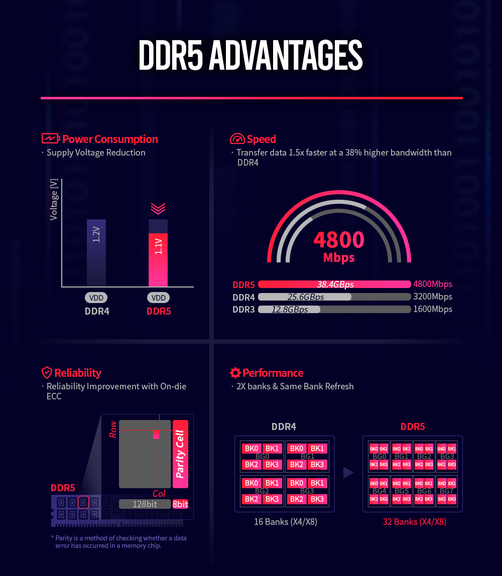
SK Hynix had previously been working on its DDR5-6400 DRAM, which has 16 Gb which is formed of 32 banks, with 8 bank groups, with double the available bandwidth and access potential when compared with DDR4-3200 memory. For reference, DDR4 uses 16 banks with 4 bank groups. The key solution to improve access throughout is the burst length, which has been doubled to 16 when compared with 8 on DDR4. Another element to consider is DDR4 can't by proxy run operations while it's refreshing. DDR5 is using SBRF (same bank refresh function) which allows the system the ability to use other banks while one is refreshing, which in theory improves memory access availability.
As we've already mentioned, SK Hynix already has DDR5-6400 in its sights which are built upon its second-generation 10nm class fabrication node. SK Hynix has now listed that it plans to develop up to DDR5-8400. Similar in methodology to its DDR5-6400 DRAM, DDR5-8400 requires much more forethought and application. What's interesting about SK Hynix's DDR5-8400 is the jump in memory banks, with DDR5-8400 using 32 banks, with 8 bank groups.
Not just content at increasing overall memory bandwidth and access performance over DDR4, the new DDR5 will run with an operating voltage of 1.1 V. This marks a 9% reduction versus DDR4's operating voltage which is designed to make DDR5 more power-efficient, with SK Hynix reporting that it aims to reduce power consumption per bandwidth by over 20% over DDR4.
To improve performance and increase reliability in server scenarios, DDR5-8400 will use on-die ECC (Error Correction) and ECS (Error Check and Scrub) which is a milestone in the production of DDR5. This is expected to reduce overall costs, with ECS recording any defects present and sends the error count to the host. This is designed to improve transparency with the aim of providing enhanced reliability and serviceability within a server system. Also integrated into the design of the DDR5-8400 DRAM is Decision Feedback Equalization (DFE), which is designed to eliminate reflective noise when running at high speeds. SK Hynix notes that this increases the speed per pin by a large amount.
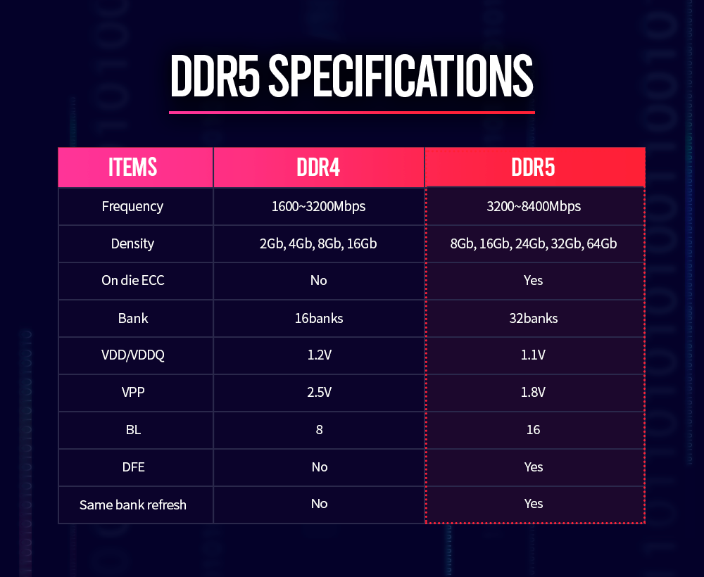
In the above image from specification comparison between DDR4 and DDR5 from SK Hynix, one interesting thing to note is that it mentions DRAM chips with density up to 64 gigabit. We already know that the chip size of DDR5 is 65.22mm², with a data rate of 6.4 Gbps per pin, and uses its 1y-nm 4-metal DRAM manufacturing process. It is worth pointing out that the DDR5-5200 RDIMM we reported on back in November 18, uses 16 Gb DRAM chips, with further scope to 32 Gb reported. SK Hynix aims to double this to 64 Gb chips which do double the density, at lower power with 1.1 volts.
Head of DRAM Product Planning at SK Hynix, Sungsoo Ryu stated that:
"In the 4th Industrial Revolution, which is represented by 5G, autonomous vehicle, AI, augmented reality (AR), virtual reality (VR), big data, and other applications, DDR5 DRAM can be utilized for next-gen high-performance computing and AI-based data analysis".
SK Hynix if still on schedule with the current Coronavirus COVID-19 pandemic, looks set to enter mass production of DDR5 later this year.
Related Reading
Source: SK Hynix


84 Comments
View All Comments
mode_13h - Saturday, April 4, 2020 - link
You think only about consumer.With their memory controller(s) on a separate I/O die, AMD could support DDR4 on consumer platforms and DDR5 in EPYC.
Valantar - Sunday, April 5, 2020 - link
Sure, that's possible, but it also doesn't matter for anyone outside of datacentres. For most tech enthusiasts, what they said is quite likely to be true.ET - Sunday, April 5, 2020 - link
It's possible that AMD will offer a different I/O die with DDR5. Chiplets certainly allow for this. That said, my guess would be that the first DDR5 support will be in Cézanne. I expect laptops of next year to support LPDDR5, and AMD is hopefully getting ready for this.Valantar - Sunday, April 5, 2020 - link
... LPDDR4X support arrived in late 2019/ early 2020 for PCs after being officially launched in early 2017. What is causing your extreme optimism as to the uptake of LPDDR5 in PC SoCs?bill.rookard - Friday, April 3, 2020 - link
Ok, on-Die ECC. Does that mean that the DRAM DIMMs have the ability to perform their own ECC functions, and just inform the OS about ECC corrections? Would that also mean that you're separating ECC from the motherboards and that it's now only limited by OS support?If so - that would be amazing - it would simplify things and make them more reliable across the board.
mode_13h - Friday, April 3, 2020 - link
> Does that mean that the DRAM DIMMs have the ability to perform their own ECC functions, and just inform the OS about ECC corrections?That's the way I read it.
> Would that also mean that you're separating ECC from the motherboards and that it's now only limited by OS support?
With history as a guide, I'm guessing that on-die ECC is an optional feature that you won't get in typical consumer memory.
Also, there should be some parity on the link, itself, which probably won't be implemented on mainstream consumer boards.
ikjadoon - Friday, April 3, 2020 - link
On-die ECC for consumer workloads *actually* has some benefits, particularly for lowering power draw. Micron gave a presentation on this some years ago:https://www.micron.com/about/blog/2017/february/th...
Direct download of the white paper: https://www.micron.com/-/media/client/global/docum...
Slightly higher active power usage for far, far, far more efficient standby (i.e., refresh) power usage.
"Because the refresh rates are set very conservatively, a DRAM with ECC can be refreshed
at a rate approximately one quarter of what is set forth in the specification."
Valantar - Saturday, April 4, 2020 - link
I also get the impression that on-die ECC is (partly) there to make it easier to run these chips at absurdly high data rates - or is that just the pessimist in me talking?Also, @mode_13h, couldn't on-die ECC be entirely transparent to the OS? As long as the OS gets the data it needs, does it matter to it whatsoever if ECC corrected anything or not?
mode_13h - Saturday, April 4, 2020 - link
Of course the OS doesn't *need* to be involved, but you'd ideally like it to mark the page as bad, in case another bit starts flipping, as well. That's just one example.But that's not really any different to the situation where the CPU's own memory controller is doing the ECC, which is the situation we have today.
mode_13h - Saturday, April 4, 2020 - link
Okay, so maybe it'll be enabled for DDR5L?I'm still not assuming it'll be the default for consumer desktop memory.