SiPearl Lets Rhea Design Leak: 72x Zeus Cores, 4x HBM2E, 4-6 DDR5
by Andrei Frumusanu on September 8, 2020 9:00 AM EST
In what seems to be a major blunder by the SiPearl PR team, a recent visit by a local French politician resulted in the public Twitter posting in what looks like the floor plan of the company’s first-generation server chip project “Rhea”.
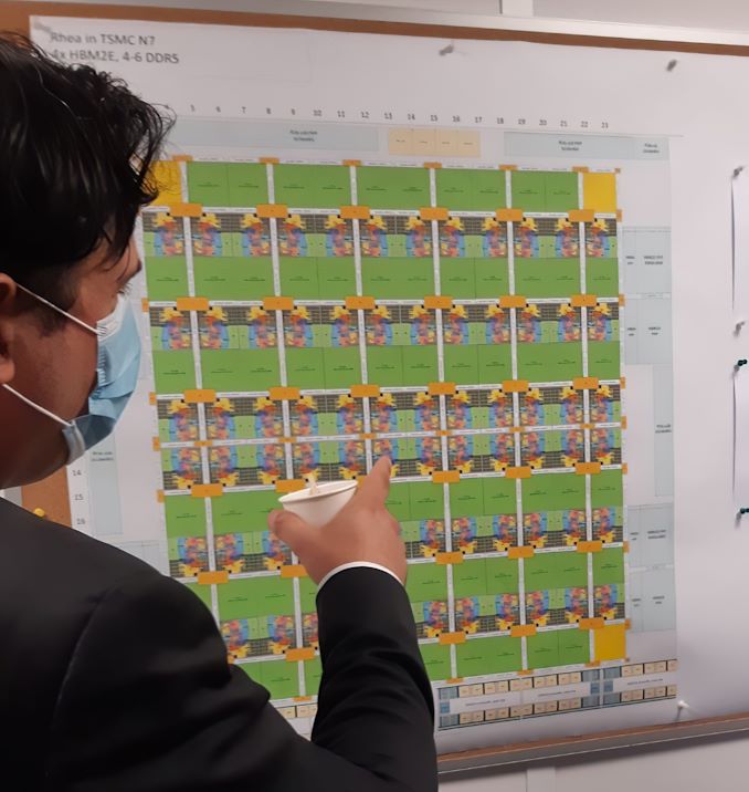
During a visit of Alexandra Dublanche, a local Île-de-France politician and vice president of economic development and other responsibilities for the region, the PR teams had made some photo-op captures of a tour of the office. Amongst the published pictures includes a shot of the company’s Rhea server chip project with some new, until now unreleased details of the European Processor Initiative-backed project.
Accélérer le développement européen de microprocesseurs à haute performance est un enjeu de souveraineté 🇪🇺
— Alexandra Dublanche (@ADublanche) September 8, 2020
C’est le défi auquel s’attaque la pépite technologique @SIPEARL_SAS basée à #MaisonsLaffitte en @iledefrance
La Région sera à ses côtés face à cet enjeu majeur! pic.twitter.com/kcBwghlfsP
In a close-up and up-scaling of the image, we can see that it’s a detailed floor-plan of the server SoC Rhea, labelled for a target TSMC 7nm process.
We can detail 72 CPU cores and 68 mesh network L3 cache slices in the floor plan, surrounded by various IP whose labels are too small to be legible. SiPearl had previously confirmed that the project uses Arm’s upcoming Neoverse “Zeus” cores which succeed the Neoverse N1 Ares cores that are being used in current generation Arm server SoC designs such as Amazon’s Graviton2 or Ampere’s Altra.
Beyond the confirmation of a core-count, we also see that the Rhea design sports a high-end memory subsystem, with the floor plan labelled as having 4x HBM2E controllers and 4-6 DDR5 controllers. Such a hybrid memory system would allow for extremely high bandwidth to be able to feed such a large number of cores, while still falling back to regular DIMMs to be able to scale in memory capacity.
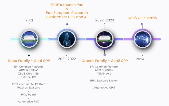
The Rhea family of processors is roadmapped to come to market in 2021. The only curious divergence here is that SiPearl previously stated that this was an N6 project, whilst the recent Twitter picture states it being N7. Given that both processes are design compatible, it might just be a recent shift in the project, or the company still plans to productise it in the N6 node when it comes to market.
The design’s aggressive memory subsystem with the inclusion of HBM2E points out that the company is aiming for quite high performance targets, joining the ranks of Fujitsu in terms of designing a CPU with advanced HBM memory.
Related Reading:
- European Processor Initiative Backed SiPearl Announces Licensing of Arm Zeus Neoverse CPU IP
- Amazon's Arm-based Graviton2 Against AMD and Intel: Comparing Cloud Compute
- Next Generation Arm Server: Ampere’s Altra 80-core N1 SoC for Hyperscalers against Rome and Xeon
- Ampere’s Product List: 80 Cores, up to 3.3 GHz at 250 W; 128 Core in Q4
- A Success on Arm for HPC: We Found a Fujitsu A64FX Wafer
- New #1 Supercomputer: Fugaku in Japan, with A64FX, take Arm to the Top with 415 PetaFLOPs


27 Comments
View All Comments
Richard Trauben - Thursday, September 10, 2020 - link
micron dropped support. hbm banndwidth is ~10X hmc.roadmap.hbm: 128 bytes @ single digit GHZ. pinout w/in package.
hmb: <1 byte @ tens of GHz..pinout leaves package.
Santoval - Wednesday, September 16, 2020 - link
HBM killed it..Wilco1 - Tuesday, September 8, 2020 - link
Slow Atom cores with bolted on AVX512 at just 1.4GHz never was a good idea. People did take notes indeed - A64FX is about 2.5 times as fast as Xeon Phi and 4 times more power efficient.Given Zeus will be even faster than Neoverse N1, it should be ridiculously quick. With 72 cores it'll beat EPYC 2 and 3. Making super computers out of cores this fast actually makes sense.
Spunjji - Wednesday, September 9, 2020 - link
Exactly that. The problem with the Larrabee project right from the start was using the wrong tools for the wrong jobs. Until now Intel has only ever really had an x86 hammer (ignoring the Itanic), so they treat every problem like an x86 nail.Wilco1 - Wednesday, September 9, 2020 - link
And then the nail fails as expected and gets cancelled... Anyone remember Quark? Using an ancient 80486 to enter the microcontroller market was just insanity and proof Intel completely lost its marbles.TeXWiller - Wednesday, September 9, 2020 - link
Maybe Intel used the Quark SBC projects as a public beta test for the later inclusion in their PCHs as the ME and the Innovation Engine. But claiming that publicly would be just paranoid. =)There is a pattern of continuous integration here though, as always for Intel. One could see the Phi being already a part of Xeon architecture, particularly so in the light of the heavy AVX512 clock frequency offsets. That certainly would solve the Phi's issue with high bandwidth network related processing in certain workloads which was an issue Mellanox marketing could drill into.
Duncan Macdonald - Tuesday, September 8, 2020 - link
HBM2E has similar latency to ordinary DRAM and a much higher bandwidth (>400GB/sec stack and 4 stacks for this design giving a possible bandwidth of >1.6TB/sec). HBM2E capacity is lower than standard DRAM - max so far is 16GB per stack giving a maximum total of 64GB for this design. The HBM2E stacks are best thought of as local storage (somewhat like a huge L4 cache) for arrays and data that is very frequently accessed.High capacity DRAM is normally slower as large DIMMs (eg 256GB) need buffering circuits due to the number of chips on the DIMM and even without that the bandwidth per DDR4 channel (under 30GB/sec) is less than one tenth of the bandwidth of an HBM2E stack.
Tabalan - Tuesday, September 8, 2020 - link
Hmm, any info when Zeus will be released (it's A77 ? N1 core was announced 1,5 year ago and still no leaks about N2. Cortex A series gets new core every year, hoped for same schedule for servers.In this news ( https://www.anandtech.com/show/15738/epi-backed-si... ) SiPearl expects to release Zeus based SoC in 2022, it's so so far away...
anonomouse - Tuesday, September 8, 2020 - link
Appears that it’ll be announced at Arm Dev summit next month.Tabalan - Tuesday, September 8, 2020 - link
Thanks.Btw, can we get edit button please? It would be helpful against effects of momentary brain fart.