DDR5 is Coming: First 64GB DDR5-4800 Modules from SK Hynix
by Dr. Ian Cutress on October 6, 2020 8:00 AM EST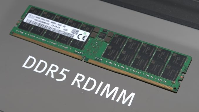
Discussion of the next generation of DDR memory has been aflutter in recent months as manufacturers have been showcasing a wide variety of test vehicles ahead of a full product launch. Platforms that plan to use DDR5 are also fast approaching, with an expected debut on the enterprise side before slowly trickling down to consumer. As with all these things, development comes in stages: memory controllers, interfaces, electrical equivalent testing IP, and modules. It’s that final stage that SK Hynix is launching today, or at least the chips that go into these modules.
DDR5 is the next stage of platform memory for use in the majority of major compute platforms. The specification (as released in July 2020) brings the main voltage down from 1.2 V to 1.1 V, increases the maximum silicon die density by a factor 4, doubles the maximum data rate, doubles the burst length, and doubles the number of bank groups. Simply put, the JEDEC DDR specifications allows for a 128 GB unbuffered module running at DDR5-6400. RDIMMs and LRDIMMs should be able to go much higher, power permitting.
| JEDEC DDR Generations | ||||||
| DDR5 | DDR4 | DDR3 | LPDDR5 | |||
| Max Die Density | 64 Gbit | 16 Gbit | 4 Gbit | 32 Gbit | ||
| Max UDIMM Size (DSDR) |
128 GB | 32 GB | 8 GB | N/A | ||
| Max Data Rate | 6.4 Gbps | 3.2 Gbps | 1.6 Gbps | 6.4Gbps | ||
| Channels per Module | 2 | 1 | 1 | 1 | ||
| Total Width (Non-ECC) |
64-bits (2x32-bit) |
64-bits | 64-bits | 16-bits | ||
| Banks (Per Group) |
4 | 4 | 8 | 16 | ||
| Bank Groups | 8/4 | 4/2 | 1 | 4 | ||
| Burst Length | BL16 | BL8 | BL8 | BL16 | ||
| Voltage (Vdd) | 1.1v | 1.2v | 1.5v | 1.05v | ||
| Vddq | 1.1v | 1.2v | 1.5v | 0.5v | ||
There are four angles in the world of DDR that everyone involved in the specification wants to iterate on. Capacity is the obvious one, but also memory bandwidth plays a key role in performance scaling of common multi-core workloads in the large core-count servers we are seeing. The other two are power (an obvious goal), and the other is latency, another key metric for performance.
With DDR5, one of the major changes to help drive this is the way the memory is seen by the system. Rather than being a single 64-bit data channel per module, DDR5 is seen as two 32-bit data channels per module (or 40 bits in ECC). The burst length has doubled, meaning that each 32-bit channel will still deliver 64 bytes per operation, but can do so in a more interleaved fashion. That means the standard ‘two 64-bit channel DDR4’ system will morph into a ‘quad 32-bit channel DDR5’ arrangement, although each memory stick provides a total of 64-bits but in a more controllable way. This also makes doubling the data rate, a key element in increasing peak bandwidth, easier, as well as a finer-grained bank refresh feature, which allows for asynchronous operations on the memory while it is in use, reducing latency.
Voltage regulation is also being moved from the motherboard to the memory module, allowing the module to regulate its own needs. We already saw DDR4 adopt a per-chip Vdroop control, but this takes the whole idea a stage further for tighter power control and management. It also puts power management in the hands of the module vendor rather than the motherboard manufacturer, allowing the module manufacturer to size up what is required for faster memory – it will be interesting to see how different firmware cope with non-JEDEC standard gaming memory that will undoubtedly go above specification.
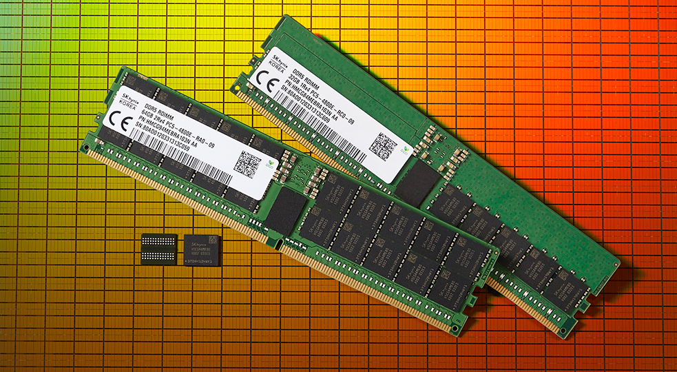
SK Hynix’s announcement today is that they are ready to start shipping DDR5 ECC memory to module manufacturers – specifically 16 gigabit dies built on its 1Ynm process that support DDR5-4800 to DDR5-5600 at 1.1 volts. With the right packaging technology (such as 3D TSV), SK Hynix says that partners can build 256 GB LRDIMMs. Additional binning of the chips for better-than-JEDEC speeds will have to be done by the module manufacturers themselves. SK Hynix also appears to have its own modules, specifically 32GB and 64GB RDIMMs at DDR5-4800, and has previously promised to offer memory up to DDR5-8400.
SK Hynix has not provided information of the sub-timings of these modules. The JEDEC specification defines three different modes for DDR5-4800:
- DDR5-4800A: 34-34-34
- DDR5-4800B: 40-40-40
- DDR5-4800C: 42-42-42
It is unclear which one of these that SK Hynix is using. The module says '4800E', however that appears to just be part of the module naming, as the JEDEC specification doesn't go beyond a CL value of 42 for DDR5-4800.
For bandwidth, other memory manufacturers have quoted that for the theoretical 38.4 GB/s that each module of DDR5-4800 can bring, they are already seeing effective numbers in the 32 GB/s range. This is above the effective 20-25 GB/s per channel that we are seeing on DDR4-3200 today. Other memory manufacturers have already announced that they are sampling DDR5 with customers since the beginning of the year.
As part of the announcement, it was interesting to see Intel as one of the lead partners for these modules. Intel has committed to enabling DDR5 on its Sapphire Rapids Xeon processor platform, due for initial launch in late 2021/2022. AMD was not mentioned with the announcement, and neither were any Arm partners.
SK Hynix quotes that DDR5 is expected to be 10% of the global market in 2022, increasing to 43% in 2024. The intersection point for consumer platforms is somewhat blurred at this point, as we’re probably only half-way through (or less than half) of the DDR4 cycle. Traditionally we expect a cost interception between old and new technology when they are equal in market share, however the additional costs in voltage regulation that DDR5 requires is likely to drive up module costs – scaling from standard power delivery on JEDEC modules up to a beefier solution on the overclocked modules. It should however make motherboards cheaper in that regard.
Source: SK hynix
Related Reading
- DDR5 Memory Specification Released: Setting the Stage for DDR5-6400 And Beyond
- SK Hynix: We're Planning for DDR5-8400 at 1.1 Volts
- Cadence DDR5 Update: Launching at 4800 MT/s, Over 12 DDR5 SoCs in Development
- Samsung to Produce DDR5 in 2021 (with EUV)
- Here's Some DDR5-4800: Hands-On First Look at Next Gen DRAM
- CES 2020: Micron Begins to Sample DDR5 RDIMMs with Server Partners
- SK Hynix Details DDR5-6400
- Keysight Reveals DDR5 Testing & Validation System
- SK Hynix Develops First 16 Gb DDR5-5200 Memory Chip, Demos DDR5 RDIMM
- Cadence & Micron DDR5 Update: 16 Gb Chips on Track for 2019
- Cadence and Micron Demo DDR5-4400 IMC and Memory, Due in 2019


42 Comments
View All Comments
kepstin - Friday, February 19, 2021 - link
The thing that matters here isn't the number of channels, but rather the width (number of bits) of the memory interface.Current consumer CPUs have a 128bit memory bus, so you use pairs of DDR4 DIMMs which provide a 64bit memory bus each for a total of 2×64bit
Future consumer CPUs will probably still have a 128bit memory bus, so you will use pairs of DDR5 DIMMs which each provide two 32bit memory busses for a total of 4×32bit.
lorribot - Sunday, October 18, 2020 - link
In the consumer space this will be troubling for AMD. Intel cares little about backwards compatibility and will therefor just create a new socket and all that But AMD has made a big play about AM4 sockets for all it processors but none of the old processors will be able to run DDR5 and the new processors will not be able support DDR4 and 5 due to the changes in power for DDR5 and the controller changes, so AMD will either have to produce two processors, one AM4 DDR4 and one DDR5 and new chipsets, so they may as well do a new socket and will likely get a big pasting over it. Maybe a good time to go all in on PCIe 5 as well.