The Snapdragon 888 vs The Exynos 2100: Cortex-X1 & 5nm - Who Does It Better?
by Andrei Frumusanu on February 8, 2021 3:00 AM EST- Posted in
- Mobile
- Samsung
- Qualcomm
- Smartphones
- SoCs
- Snapdragon 888
- Exynos 2100
5nm / 5LPE: What do we know?
Starting off with the biggest new change of this generation, both the Snapdragon 888 and the Exynos 2100 are manufactured on Samsung’s new 5nm process node, which is the biggest unknown in today’s comparison.
What’s important to remember is that although Samsung calls this node 5nm, its design and characteristics are more similar to that of their 7nm node. Key new characteristics of the new node here are the reintroduction of single diffusion breaks (SDB) on an EUV process node, as well as slight changes in the cell libraries of the process.
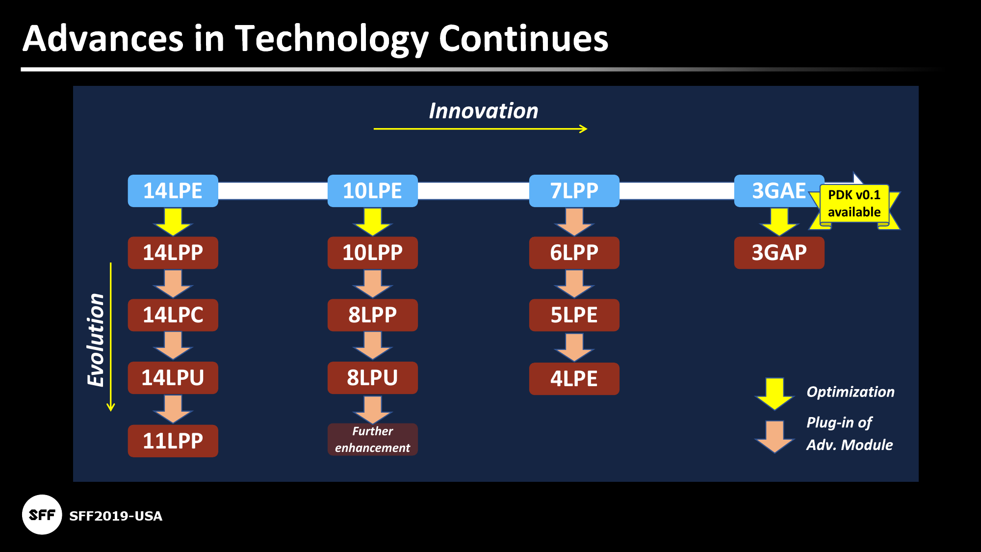
| Advertised PPA Improvements of New Process Technologies Data announced by companies during conference calls, press briefings and in press releases |
||||||
| 7LPP vs 10LPE |
6LPP vs 7LPP |
5LPE vs 7LPP |
3GAE vs 7LPP |
|||
| Power | 50% | lower | 20% | 50% | ||
| Performance | 20% | ? | 10% | 35% | ||
| Area Reduction | 40% | ~9% | <20% | 40% | ||
Per Samsung’s own numbers, the foundry claims that 5LPE is either 20% lower power than 7LPP, or 10% more performance. These are actually quite important figures to put into context, particularly when we’re comparing designs which are manufactured on TSMC’s process nodes.
In least year’s review of the Galaxy S20 series and the Exynos 990 and Snapdragon 865 SoCs, an important data-point that put things into context was Qualcomm’s Snapdragon 765 SoC which was also manufactured on Samsung’s 7LPP node, and featuring Cortex-A76 cores. In that comparison we saw that The Exynos 990 and the Snapdragon 765’s A76 cores behaves very similarly in terms of power consumption, however they fell behind TSMC-based Cortex-A76 cores by anywhere from 20% to 30%.
In that context, Samsung’s 5LPE process node improving power by 20% would mean they’d only be catching up with TSMC’s 7nm nodes.
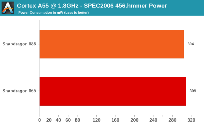
An interesting comparison to make – and probably one of the rare ones we’re actually able to achieve today, is the comparison between the Cortex-A55 cores inside of both the Snapdragon 865 and the new Snapdragon 888. Both SoCs feature the same IP cores, clock them at the same 1.8GHz frequency, and both feature the same amount of L2 cache, with their only real difference being their process nodes.
Using SPEC’s 456.hmmer – because it’s a workload that primarily resides in the lower cache hierarchies and thus, we avoid any impact of the possibly different memory subsystem, we can see that both SoCs’ power consumption indeed is almost identical, with performance also being identical with a score of 6.84 versus 6.81 in favour of the new Snapdragon 888.
So at least at first glance, our theory that Samsung’s 5LPE merely just catches up with the power consumption and power efficiency of TSMC’s N7/N7P nodes seems to be valid – at least at these frequencies.

Further interesting data is the voltage curves of the CPUs on the Exynos 2100. I’ve extracted the frequency voltages tables of both my devices, a regular S21 and an S21 Ultra, with the above curves being the better binned chip inside of the smaller S21.
Generationally, Samsung seems to have been able to greatly reduce voltages this generation. On the Cortex-A55 cores, the cores now only require 800mV at 2GHz whilst the Exynos 990 last year in our review unit they required over 1050mV. Similarly, although the comparison isn’t apples-to-apples, the Cortex-A78 cores at 2.5GHz only require 862mV, while the Cortex-A76 cores of the previous generation required also 1050mV.
What’s also very interesting to see is the voltage curves of the Cortex-X1 cores versus the Cortex-A78 cores: they’re both nigh identical to each other, which actually lines up with Arm’s claims that the new X1 cores have the same frequency capabilities as the A78 cores, only being larger and increasing their power consumption linearly in relation to their frequency.
Samsung’s frequency tables indicate that they had been testing the A55 up to 2.6GHz, and the X1 and A78 cores up to 3.2GHz – however voltages here are quite higher and it’s also likely SLSI wouldn’t have been able to achieve similar chip yields.
Unfortunately, I wasn’t able to extract data from my Snapdragon 888 S21 Ultra, so I can’t tell exactly where it falls in terms of voltages compared to the Exynos 2100. One thing I can confirm as being quite different between the two SoCs is that Samsung does actually give the Exynos 2100’s Cortex-X1 core its own dedicated voltage rail and PMIC regulator, while the Snapdragon 888 shares the same voltage rail across the X1 and A78 cores. In theory, that could mean that in more mixed-thread workloads, the Exynos has the opportunity to be more power efficiency than the Snapdragon 888.
Generally, the one thing I want people to take away here is that although Samsung calls this their 5nm node, it’s quite certain that it will not perform the same as TSMC’s 5nm node. Usually we don’t care about density all too much, however performance and power efficiency are critical aspects that effect the silicon and the end-products’ experiences.


123 Comments
View All Comments
Archer_Legend - Tuesday, February 9, 2021 - link
Actually samsung has still M6 cores in its belly, the development team was shut down only after they completed the M6 cores.Difficoult to say if they would have been better than an X1.
However it seems that arm has rushed this whole a78 and X1 thing and samsung rushed to put too much stuff in the cpu with evidently not enough time to do it well
watzupken - Monday, February 8, 2021 - link
Feels like a 20nm all over again. The move to Samsung's fab certainly did not help with the new SD 888 and Samsung's Exynos is able to close the performance gap since they are on the same node. In fact, this review also somewhat confirmed that Nvidia's jump to Samsung's 8nm certainly contributed to the high power consumption and lower clockspeed.s.yu - Monday, February 8, 2021 - link
That would be saying Samsung's 8nm is worse than TSMC 12nm, it's not that bad, it should be a bit better than TSMC 10nm.Spunjji - Monday, February 8, 2021 - link
I assumed they meant higher power relative to TSMC 7nm - of course overall power is still a little higher than Turing on TSMC 12nm because of the higher logic density.Otritus - Monday, February 8, 2021 - link
Samsung's 8nm is based on their 10nm, and can be considered a more refined variant with about a 10% improvement in efficiency. TSMC's 12nm is based on their 16 nm, with about the same efficiency improvements. 10lpp vs 14lpp is about 40% less power. 14lpp was computed to be about 25% less efficient than 16ff+. Which would mean 8lpp has around 20% lower power consumption than 16ff+. Tsmc 10nm should be around 40% less power than 16ff+, so Samsung 8nm is in fact worse than Tsmc 10nm.Silver5urfer - Monday, February 8, 2021 - link
Samsung 8nm for Nvidia doesn't have much impact in the Desktop PEG scene. Because the GPUs are already heavy on power consumption. Having a TSMC will make it efficient but it won't help with temps / clocks or the performance, always a new node helps with either get perf boost or efficiency.Nvidia wanted cheap manufacturing for it's GPUs and more volume. But the latter is busted due to artificially pumping up this BS by Mining craze & corona problem. That's why A100 is on TSMC 7N instead of Samsung, because HPC and other hyperscalers need efficiency.
In mobile it matters a lot due to the stupid Li Ion garbage tech.
Otritus - Monday, February 8, 2021 - link
Efficiency for desktop gpus matters a lot. At best you are limited by temperature and noise, at worst you are also limited by power consumption (primarily oem pcs). If a cooler can dissipate 375 watts at an acceptable noise and temperature threshold, then that's the max power the gpu can ship at(the ceiling is lower if overclocking headroom is considered).Switching to tsmc will help temperatures, performance, and clock. Lower power consumption means lower temperatures. The tsmc node can also clock higher which drives performance up. If using tsmc allows the chip to clock n% higher at the same power, ship it with n/2% more frequency, and now performance and oc headroom is higher, and temps and power draw are lower.
Spunjji - Thursday, February 11, 2021 - link
Both of the major manufacturer's top-end GPUs are limited by power input and heat dissipation - that's why they rarely perform much better than the next tier down, despite having significantly more execution resources. They do better on a performance-per-watt basis, though, because they're operating at a more sane part of the efficiency curve.geoxile - Monday, February 8, 2021 - link
Tsmc 12/16nm was roughly on par with Samsung 14nm.melgross - Monday, February 8, 2021 - link
Yes, when Apple split its SoC production between Samsung and TSMC that one year when they were looking to replace Samsung with TSMC, it was found here, and in other places, that TSMC’ s larger process was 20% more power efficient than Samsung’s smaller process. I think it was the 14 node for Samsung and the 16 for TSMC.So nothing seems to have changed. Samsung’s process technology remains inferior to that of TSMC.