NVIDIA Unveils PCIe version of 80GB A100 Accelerator: Pushing PCIe to 300 Watts
by Ryan Smith on June 28, 2021 8:00 AM EST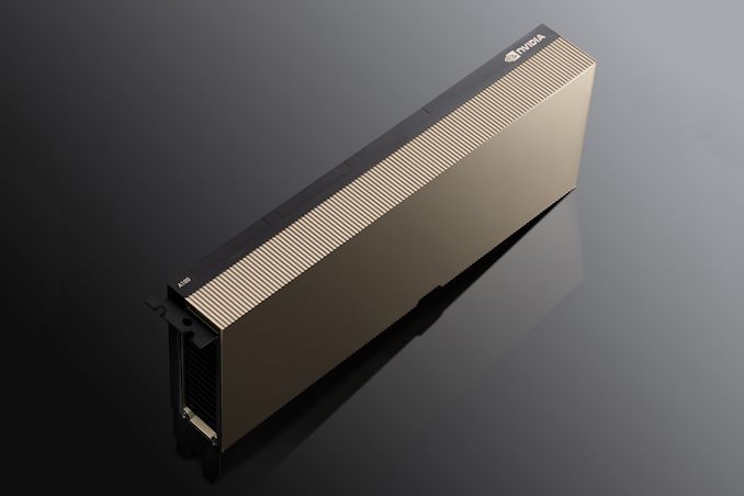
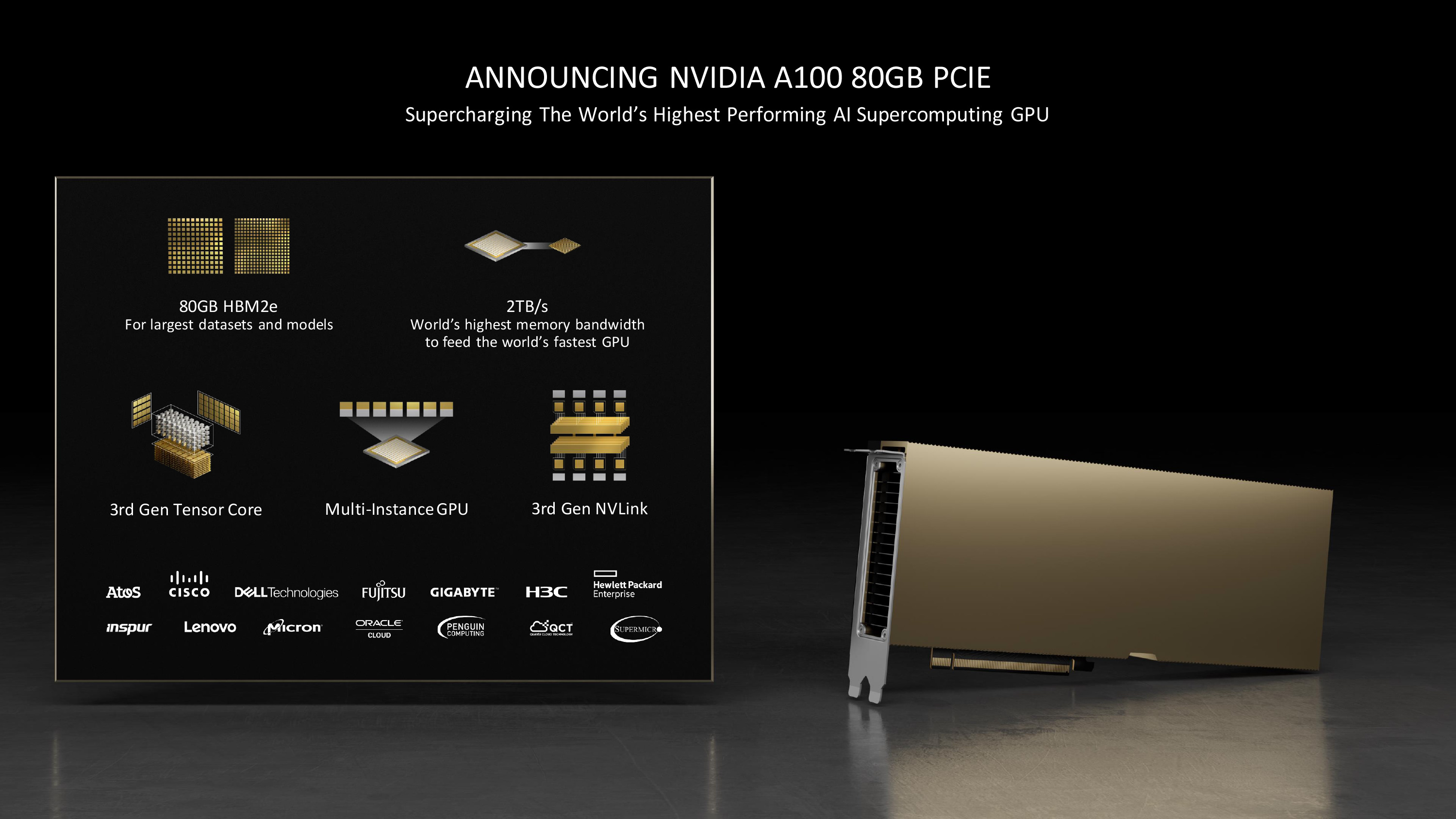
As part of today’s burst of ISC 2021 trade show announcements, NVIDIA this morning is announcing that they’re bringing the 80GB version of their A100 accelerator to the PCIe form factor. First announced in NVIDIA’s custom SXM form factor last fall, the 80GB version of the A100 was introduced to not only expand the total memory capacity of an A100 accelerator – doubling it from 40GB to 80GB – but it also offered a rare mid-generation spec bump as well, cranking up the memory clockspeeds by a further 33%. Now, after a bit over 6 months, NVIDIA is releasing a PCIe version of the accelerator for customers who need discrete add-in cards.
The new 80GB version of the PCIe A100 joins the existing 40GB version, and NVIDIA will continue selling both versions of the card. On the whole, this is a pretty straightforward transfer of the 80GB SMX A100 over to PCIe, with NVIDIA dialing down the TDP of the card and the number of exposed NVLinks to match the capabilities of the form factor. The release of the 80GB PCIe card is designed to give NVIDIA’s traditional PCIe form factor customers a second, higher-performing accelerator option, particularly for those users who need more than 40GB of GPU memory.
| NVIDIA Accelerator Specification Comparison | ||||||
| 80GB A100 (PCIe) |
80GB A100 (SXM4) |
40GB A100 (PCIe) |
40GB A100 (SXM4) |
|||
| FP32 CUDA Cores | 6912 | 6912 | 6912 | 6912 | ||
| Boost Clock | 1.41GHz | 1.41GHz | 1.41GHz | 1.41GHz | ||
| Memory Clock | 3.0 Gbps HBM2 | 3.2 Gbps HBM2 | 2.43Gbps HBM2 | 2.43Gbps HBM2 | ||
| Memory Bus Width | 5120-bit | 5120-bit | 5120-bit | 5120-bit | ||
| Memory Bandwidth | 1.9TB/sec (1935GB/sec) |
2.0TB/sec (2039GB/sec) |
1.6TB/sec (1555GB/sec) |
1.6TB/sec (1555GB/sec) |
||
| VRAM | 80GB | 80GB | 40GB | 40GB | ||
| Single Precision | 19.5 TFLOPs | 19.5 TFLOPs | 19.5 TFLOPs | 19.5 TFLOPs | ||
| Double Precision | 9.7 TFLOPs (1/2 FP32 rate) |
9.7 TFLOPs (1/2 FP32 rate) |
9.7 TFLOPs (1/2 FP32 rate) |
9.7 TFLOPs (1/2 FP32 rate) |
||
| INT8 Tensor | 624 TOPs | 624 TOPs | 624 TOPs | 624 TOPs | ||
| FP16 Tensor | 312 TFLOPs | 312 TFLOPs | 312 TFLOPs | 312 TFLOPs | ||
| TF32 Tensor | 156 TFLOPs | 156 TFLOPs | 156 TFLOPs | 156 TFLOPs | ||
| Relative Performance (SXM Version) | 90%? | 100% | 90% | 100% | ||
| Interconnect | NVLink 3 12 Links (600GB/sec) |
NVLink 3 12 Links (600GB/sec) |
NVLink 3 12 Links (600GB/sec) |
NVLink 3 12 Links (600GB/sec) |
||
| GPU | GA100 (826mm2) |
GA100 (826mm2) |
GA100 (826mm2) |
GA100 (826mm2) |
||
| Transistor Count | 54.2B | 54.2B | 54.2B | 54.2B | ||
| TDP | 300W | 400W | 250W | 400W | ||
| Manufacturing Process | TSMC 7N | TSMC 7N | TSMC 7N | TSMC 7N | ||
| Interface | PCIe 4.0 | SXM4 | PCIe 4.0 | SXM4 | ||
| Architecture | Ampere | Ampere | Ampere | Ampere | ||
At a high level, the 80GB upgrade to the PCIe A100 is pretty much identical to what NVIDIA did for the SXM version. The 80GB card’s GPU is being clocked identically to the 40GB card’s, and the resulting performance throughput claims are unchanged.
Instead, this release is all about the on-board memory, with NVIDIA equipping the card with newer HBM2E memory. HBM2E is the informal name given to the most recent update to the HBM2 memory standard, which back in February of this year defined a new maximum memory speed of 3.2Gbps/pin. Coupled with that frequency improvement, manufacturing improvements have also allowed memory manufacturers to double the capacity of the memory, going from 1GB/die to 2GB/die. The net result being that HBM2E offers both greater capacities as well as greater bandwidths, two things which NVIDIA is taking advantage of here.
With 5 active stacks of 16GB, 8-Hi memory, the updated PCIe A100 gets a total of 80GB of memory. Which, running at 3.0Gbps/pin, works out to just under 1.9TB/sec of memory bandwidth for the accelerator, a 25% increase over the 40GB version. This means that not only does the 80GB accelerator offer more local storage, but rare for a larger capacity model, it also offers some extra memory bandwidth to go with it. That means that in memory bandwidth-bound workloads the 80GB version should be faster than the 40GB version even without using its extra memory capacity.
This additional memory does come at a cost, however: power consumption. For the 80GB A100 NVIDIA has needed to dial things up to 300W to accommodate the higher power consumption of the denser, higher frequency HBM2E stacks. This is a very notable (if not outright surprising) change in TDPs due to the fact that NVIDIA has long held the line for its PCIe compute accelerators at 250W, which is broadly considered the limits for PCIe cooling. So a 300W card not only deviates from NVIDIA’s past cards, but it means that system integrators will need to find a way to provide another 50W of cooling per card. This isn’t something I expect to be a hurdle for too many designs, but I definitely won’t be surprised if some integrators continue to only offer 40GB cards as a result.
And even then, the 80GB PCIe A100 would seem to be held back a bit by its form factor. The 3.0Gbps memory clock is 7% lower than the 80GB SXM A100 and its 3.2Gbps memory clock. So NVIDIA is apparently leaving some memory bandwidth on the table just to get the card to fit in the expanded 300W profile.
On that note, it doesn’t appear that NVIDIA has changed the form factor of the PCIe A100 itself. The card is entirely passively cooled, designed to be used with servers with (even more) powerful chassis fans, and fed by dual 8-pin PCIe power connectors.
With regards to overall performance expectations, the new 80GB PCIe card should trail the SXM card in a similar fashion as the 40GB models. Unfortunately, NVIDIA’s updated A100 datasheet doesn’t include a relative performance metric this time around, so we don’t have any official figures for how the PCIe card will compare to the SXM card. But, given the continued TDP differences (300W vs 400W+), I would expect that the real-world performance of the 80GB PCIe card is near the same 90% mark as the 40GB PCIe card. Which serves to reiterate that GPUs clockspeed aren’t everything, especially in this age of TDP-constrained hardware.
In any case, the 80GB PCIe A100 is designed to appeal to the same broad use cases as the SXM version of the card, which roughly boils down to AI dataset sizes, and enabling larger Multi-Instance GPU (MIG) instances. In the case of AI, there are numerous workloads which can benefit in terms of training time or accuracy by using a larger dataset, and overall GPU memory capacity has regularly been a bottleneck in this field, as there’s always someone who could use more memory. Meanwhile NVIDIA’s MIG technology, which was introduced on the A100, benefits from the memory increase by allowing each instance to be allocated more memory; running at a full 7 instances, each can now have up to 10GB of dedicated memory.
Wrapping things up, NVIDIA isn’t announcing specific pricing or availability information today. But customers should expect to see the 80GB PCIe A100 cards soon.


Source: NVIDIA


15 Comments
View All Comments
Ryan Smith - Monday, June 28, 2021 - link
The graphics-focused members of the Ampere family (GA102 and later) are on Samsung 8nm. For the compute-focused GA100, it's on TSMC.Henry223 - Monday, July 5, 2021 - link
https://surveyprize.net/This Church’s Chicken company-sponsored Church’s Chicken Survey to get valuable feedback from their consumers, which guide them to change the quality of the system and give better services to the customers.
Casper42 - Monday, June 28, 2021 - link
When do they run out of power on the "CPU 8-Pin" (ATX 12V 8pin) connector?=
Ryan Smith - Tuesday, June 29, 2021 - link
On paper? At 375W total. The card has two 8-pin connectors.UnNameless - Friday, July 9, 2021 - link
And even then the ceiling is probably higher in practice.