Intel's Process Roadmap to 2025: with 4nm, 3nm, 20A and 18A?!
by Dr. Ian Cutress on July 26, 2021 5:00 PM EST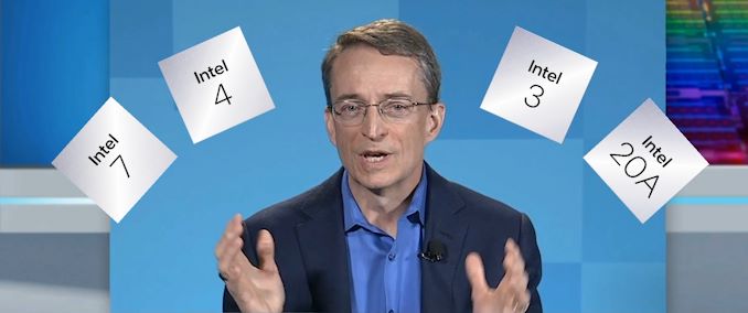
In today’s Intel Accelerated event, the company is driving a stake into the ground regarding where it wants to be by 2025. CEO Pat Gelsinger earlier this year stated that Intel would be returning to product leadership in 2025, but hasn’t yet explained how this is coming about – that is until today, where Intel has disclosed its roadmap for its next five generations of process node technology leading to 2025. Intel believes it can follow an aggressive strategy to match and pass its foundry rivals, while at the same time developing new packaging offerings and starting a foundry business for external customers. On top of all this, Intel has renamed its process nodes.
The Short Answer:
If you only take one thing away from this article, I'm going to put it here front and center. Here is what we're seeing for Intel's roadmaps, based on their disclosures today.
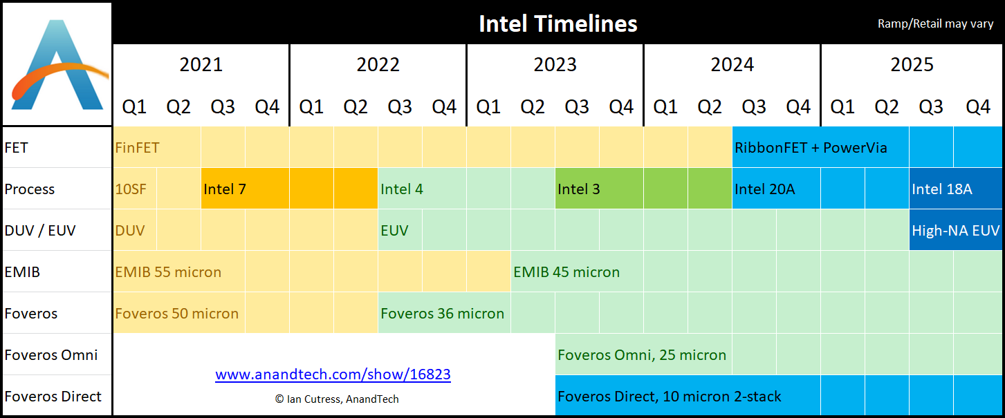
As always, there is a difference between when a technology ramps for production and comes to retail; Intel spoke about some technologies as 'being ready', while others were 'ramping', so this timeline is simply those dates as mentioned. As you might imagine, each process node is likely to exist for several years, this graph is simply showcasing the leading technology from Intel at any given time.
If you want the details on this graph, then read on.
Intel's Defines a Strong Future: Is TSMC at Risk?
Earlier this year, CEO Pat Gelsinger announced Intel’s new IDM 2.0 strategy, consisting of three elements:
- Build (7nm)
- Expand (TSMC)
- Productize (Intel Foundry Services)
The goal here is to continue to work on Intel’s process node technology development, going beyond the current 10nm designs in production today, but simultaneously using other foundry services from partners (or competitors) to regain/retain Intel’s position in its processors that drive a lot of the company revenue. The third element is IFS, Intel’s Foundry Services, where Intel is committing in a big way to opening up its manufacturing facilities to external semiconductor business.
Underpinning (1) and (3) is how Intel executes on its own process node development. While in Intel’s recent Q3 2021 earnings call CEO Gelsinger confirmed that Intel is now producing more 10nm wafers in a day than 14nm wafers, marking a shift in confidence between the two designs, it is no secret that Intel has had difficulty in transitioning from its 14nm process to its 10nm process. On June 29th this year, Intel also stated that its next generation 10nm product requires additional validation time to streamline deployment on enterprise systems for 2022. Note that at the same time, TSMC has surpassed Intel by shipping at capacity with its equivalent designs (called 7nm) and its leading edge (5nm) designs that surpass Intel’s performance.

As with the previous announcement in March, Intel is reaffirming that it intends to return to leadership performance in semiconductors in 2025. This will enable both the company to compete better as it builds its own products (1) but also offer a wider portfolio of performance and technologies for its future IFS customers (3). To do this, it is realigning the roadmap for its future process node technologies to be more aggressive with improvements, yet at the same time more modular with its technology to enable faster transitions.
Leading up this plan is Dr. Ann B Kelleher, who was named SVP and GM of the Technology Development division at Intel last year. This division is where all the research and development of Intel’s future process node technologies and enhancements comes from – it used to be part of Intel’s System Architecture Group, however it was split in July 2020 to re-establish a focus purely on Technology Development. Dr. Kelleher’s background involves process research in academia, followed by 26 years at Intel as a process engineer, moving up to managing Fab 24 in Ireland, Fab 12 in Arizona, Fab 11X in Rio Rancho, before landing in HQ in Oregon as the GM of Manufacturing and Operations.
Her experience covering both fab-scale production and process node research is going to be critical for Intel’s future plans. In discussing with Kelleher ahead of today’s announcements, she stated that she has implemented fundamental changes when it comes to supplier approach, ecosystem learnings, organizational changes, modular design strategies, contingency plans, and realigning the Technology Development Team into a more streamlined outfit ready to execute. These include key personnel such as Sanjay Natarajan as SVP and GM of Logic Development (one of Intel’s recent rehires) and Babak Sabi as CVP and GM of Assembly/Test Development
Intel is today defining ‘technology leadership by 2025’ as defined by the metric of performance per watt. We asked Intel is a pre-briefing what that means for peak performance, which is often a metric we care about for end product design, and the answer was that "peak performance remains a key part of Intel’s strategic development".
Intel Renames The Nodes: ‘Mine is Smaller’
The problem with simply posting Intel’s roadmap here is that the news is two-fold. Not only is Intel disclosing the state of its technology for the next several years, but the names of the technology are changing to better align with common industry norms.
It is no secret that having "Intel 10nm" being equivalent to "TSMC 7nm", even though the numbers actually have nothing to do with the physical implementation, has ground at Intel for a while. A lot of the industry, for whatever reason, hasn’t learned that these numbers aren’t actually a physical measurement. They used to be, but when we moved from 2D planar transistors to 3D FinFET transistors, the numbers became nothing more than a marketing tool. Despite this, every time there’s an article about the technology, people get confused. We’ve been talking about it for half a decade, but the confusion still remains.
To that end, Intel is renaming its future process nodes. Here’s the roadmap image, but I’ll be breaking it down piece by piece.
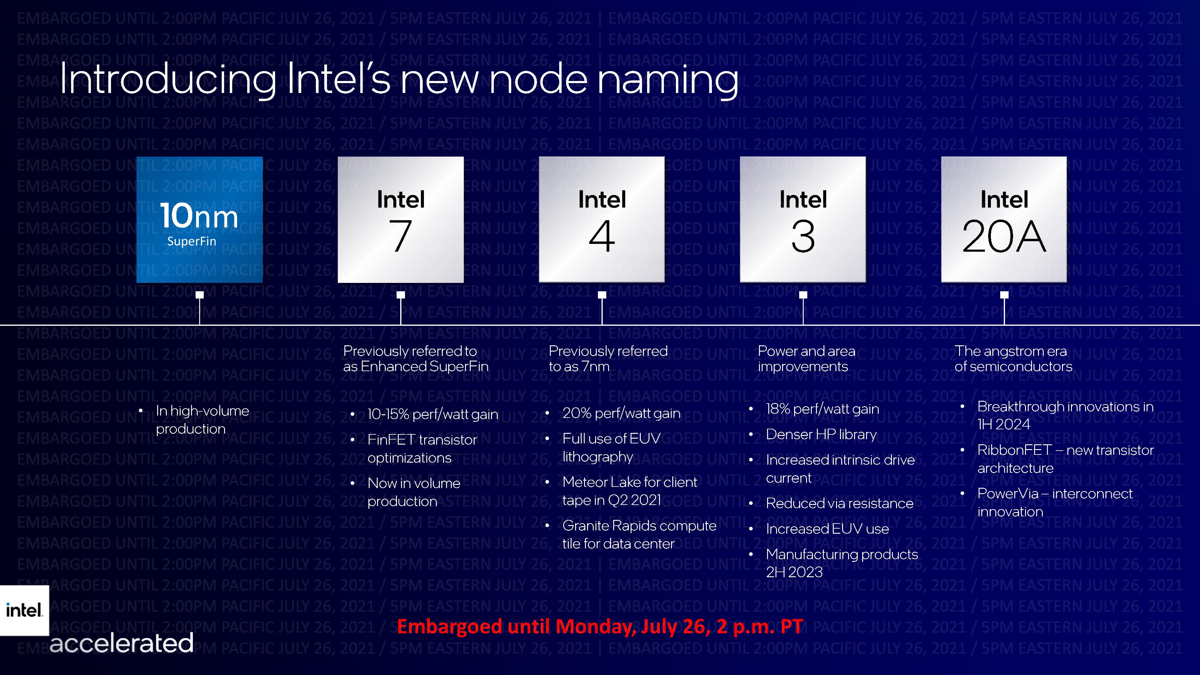
2020, Intel 10nm SuperFin (10SF): Current generation technology in use with Tiger Lake and Intel’s Xe-LP discrete graphics solutions (SG1, DG1). The name stays the same.
2021 H2, Intel 7: Previously known as 10nm Enhanced Super Fin or 10ESF. Alder Lake and Sapphire Rapids will now be known as Intel 7nm products, showcasing a 10-15% performance per watt gain over 10SF due to transistor optimizations. Alder Lake is currently in volume production. Intel’s Xe-HP will now be known as an Intel 7 product.
2022 H2, Intel 4: Previously known as Intel 7nm. Intel earlier this year stated that its Meteor Lake processor will use a compute tile based on this process node technology, and the silicon is now back in the lab being tested. Intel expects a 20% performance per watt gain over the previous generation, and the technology uses more EUV, mostly in the BEOL. Intel’s next Xeon Scalable product, Granite Rapids, will also use a compute tile based on Intel 4.
2023 H2, Intel 3: Previously known as Intel 7+. Increased use of EUV and new high density libraries. This is where Intel’s strategy becomes more modular – Intel 3 will share some features of Intel 4, but enough will be new enough to describe this a new full node, in particular new high performance libraries. Nonetheless, a fast follow on is expected. Another step up in EUV use, Intel expects a manufacturing ramp in the second half of 2023 with an 18% performance per watt gain over Intel 4.
2024, Intel 20A: Previously known as Intel 5nm. Moving to double digit naming, with the A standing for Ångström, or 10A is equal to 1nm. Few details, but this is where Intel will move from FinFETs to its version of Gate-All-Around (GAA) transistors called RibbonFETs. Also Intel will debut a new PowerVia technology, described below.
2025, Intel 18A: Not listed on the diagram above, but Intel is expecting to have an 18A process in 2025. 18A will be using ASML’s latest EUV machines, known as High-NA machines, which are capable of more accurate photolithography. Intel has stated to us that it is ASML’s lead partner when it comes to High-NA, and is set to receive the first production model of a High-NA machine. ASML recently announced High-NA was being delayed- when asked if this was an issue, Intel said no, as the timelines for High-NA and 18A are where Intel expects to intersect and have unquestioned leadership.
Intel has confirmed to us that Intel 3 and Intel 20A will be offered to foundry customers (but hasn’t stated if Intel 4 or Intel 7 will be).
To bring this altogether in a single table, with known products, we have the following:
| Intel's Process Node Technology | ||||
| Old Name | New Name | Roadmap | Products | Features |
| 10SF | 10SF | Today | Tiger Lake SG1 DG1 Xe-HPC Base Tile Agilex-F/I FPGA |
SuperMIM Thin Film Barrier Volume 10nm On sale today |
| 10ESF | Intel 7 | 2021 H2 products | Alder Lake (21) Raptor Lake (22)? Sapphire Rapids (22) Xe-HP Xe-HPC IO Tile |
10-15% PPW Upgraded FinFET ADL in Ramp today |
| 7nm | Intel 4 | 2022 H2 ramp 2023 H1 products |
Meteor Compute Tile Granite Compute Tile |
20% PPW vs 7 More EUV Silicon in Lab |
| 7+ | Intel 3 | 2023 H2 products | - | 18% PPW vs 4 Area Savings More EUV New Perf Libraries Faster Follow On |
| 5nm | Intel 20A | 2024 | - | RibbonFET PowerVia |
| 5+ | Intel 18A | 2025 | Unquestioned Leadership | 2nd Gen Ribbon High NA EUV |
One of the issues here is the difference between a process node being ready, ramping production for product launches, and actually being made available. For example, Alder Lake (now on Intel 7nm) is due to come out this year, but Sapphire Rapids is going to be more of a 2022 product. Similarly, there are reports of Raptor Lake on Intel 7 coming out in 2022 to replace Alder Lake with the tiled Meteor Lake on Intel 4 in 2023. While Intel is happy to discuss process node development time frames, product timeframes are not as open (as no doubt customers would get frustrated if the time stated is missed).
Why The Nodes Were Renamed
So as stated before, one element of renaming the nodes is due to matching parity with other foundry offerings. Both TSMC and Samsung, competitors to Intel, were using smaller numbers to compare similar density processes. With Intel now renaming itself, it gets more in-line with the industry. That being said, perhaps sneakily, Intel’s 4nm might be on par with TSMC’s 5nm, reversing the tables. By 3nm we expect there to be a good parity point, however that will depend on Intel matching TSMC’s release schedule.
Rather than throw process node names everywhere, it is typical to refer to peak quoted transistor densities instead. Here is the table we published in our recent IBM 2nm news post, but with an updated shift on Intel’s naming.
| 2021 Peak Quoted Transistor Densities (MTr/mm2) | ||||
| AnandTech Process Name |
IBM | TSMC | Intel | Samsung |
| 22nm | 16.50 | |||
| 16nm/14nm | 28.88 | 44.67 | 33.32 | |
| 10nm | 52.51 | 100.76 | 51.82 | |
| 7nm | 91.20 | 100.76 | 95.08 | |
| 5/4nm | 171.30 | ~200* | 126.89 | |
| 3nm | 292.21* | |||
| 2nm / 20A | 333.33 | |||
| Data from Wikichip, Different Fabs may have different counting methodologies * Estimated Logic Density |
||||
Exactly where Intel’s new 4nm and below will end up is yet to be disclosed, as numbers with stars alongside are based on estimates by the respective companies.
It has been expected for a while that Intel would be realigning its process node naming. Behind closed doors, I personally have been lobbying for it for a while, and I know that a few other journalists and analysts have been suggesting it to Intel as well. Some responses we received were related to apathy – one executive told me that "our customers that care about this actually know the difference", which is true for sure, but what we’re talking about here is more about perception in the wider ecosystem for enthusiasts and financial analysts who might not be up to speed. It is more or less a branding exercise, and I also told Intel that they are going to have to expect a mixed response – some voices might interpret the move as Intel trying to pull one over on the market, for example. But they’re going to have to live with it, as these are the new names.
Meanwhile, despite Intel’s struggles with 10nm, it is still a process node in production and in volume production, in use for both consumer and enterprise devices, and it's coming to desktops very soon. Even though it has some stiff competition from other players, it is still an offering in the market, and for those that want to compare process node densities using these names, it should have a moniker to avoid confusion. I am applauding that Intel is doing it sooner rather than later.
One key point to note is that the new Intel 7 node, which was formerly the 10ESF node, is not necessarily a "full" node update as we typically understand it. This node is derived as an update from 10SF, and as the diagram above states, will have ‘transistor optimizations’. Moving from 10nm to 10SF, that meant SuperMIM and new thin-film designs giving an extra 1 GHz+, however the exact details from 10SF to the new Intel 7 is unclear at this point. Intel has however stated that moving from Intel 7 to Intel 4 will be a regular full node jump, with Intel 3 using modular parts of Intel 4 with new high-performance libraries and silicon improvements for another jump in performance.
We asked Intel if these process nodes will have additional optimization points, and were told that they will – whether any of them will be explicitly productized will depend on the features. Individual optimizations may account for an additional 5-10% performance per watt, and we were told that even 10SF (which keeps its name) has had several additional optimization points that haven’t necessarily been publicized. So whether these updates get marketed as 7+ or 7SF or 4HP is not known, but as with any manufacturing process as updates occur to help improve performance/power/yield, they get applied assuming the design adheres to the same rules.
"Isn't Intel Just Trying To Pull The Wool Over Our Eyes?"
No.
The problem here is that there is no consistent node naming between foundries. Intel has been saving any number change for major advances in its node manufacturing technology, instead using +/++ to signify improvements. If we compare this to TSMC and Samsung, both of whom have been happy to give half-node jumps new numbers entirely.
For example, Samsung's 7LPP is a major node, however 6LPP, 5LPE and 4LPE are all iterative efforts on the same design (arguably also iterative of 8LPP), with 3GAE being the next major jump. Compare this to Intel, who was planning 10nm to 7nm to 5nm as major process node jumps – so while Samsung had one jump planned and 4 sub-variants (or more), Intel had two major jumps. Similarly, TSMC's 10nm was a half-node jump over 16nm, while 16nm to 7nm was the full node – Intel made 14 to 10 to 7 as full nodes.
Intel stuck to its guns a long while, and delays to 10nm effectively hurt it in a multiplicative fashion. For example, if Intel had labeled 14+ as 13nm, and 14++ as 12nm, perhaps it wouldn't be so bad. I mean, yes Intel should expect some hurt for 10nm being late, but when other foundries were showcasing smaller steps as full number jumps, it became a marketing and media nightmare. 14++++ became an industry joke, and coupled with how every time when they talked about future process nodes they had to cite the equivalent TSMC of Samsung process, it got a bit too much. It had to be explained every time, as new people come into the industry.
I've lobbied Intel to adjust its naming for a while, and I know other peers have as well. When we refer to Intel 7 from now on, we can draw equivalents to TSMC 7nm (even if TSMC is shipping 5nm in volume) without having to extensively explain differences in a simple name. This isn't Intel pulling the wool over your eyes, or trying to hide a bad situation. This is Intel catching up to the rest of the industry in how these processes are named. To add to this, it's a good thing that Intel is only renaming future nodes that haven't reached the market yet.
This is a multi-page article!
Click the dropdown below for more pages, including


326 Comments
View All Comments
Oxford Guy - Wednesday, August 11, 2021 - link
Says the person who said, in reply to one of my posts ‘we know you’re smart ... use your powers for good’.You typically post whatever sounds reasonable at a given time, no matter how inaccurate it is. I, by contrast, am capable of remembering what has been said — the positions that have been taken.
One cannot simultaneously claim I’m obviously intelligent and that my posts are valid. One cannot also post ‘agreed’ — as you did in another topic whilst pretending that my posts are vapid — unless you’re with that very vapidity.
I also find it droll that you employ the royal ‘we’ here. Are you a member of staff or merely that entitled?
Oxford Guy - Wednesday, August 11, 2021 - link
And... please — for the benefit of this forum...Learn the list of common logical fallacies. Your latest use of ad baculum is only worthy of yet another eyeroll.
mode_13h - Thursday, August 12, 2021 - link
> Says the person who said, in reply to one of my posts ‘we know you’re smart> ... use your powers for good’.
There's no logical inconsistency, there. Most of your posts seem to pull threads off-topic and offer little of value to the original subject. And quite a few are just snarky, cynical trolls.
> You typically post whatever sounds reasonable at a given time
I try to engage my brain and look at the other side of an issue, or at least from a perspective other than my narrow self-interest. And most often, what draws me to the other side of an issue is when someone takes an extreme position or makes absolutist statements that seem unjustified. If there's one thing you could say I consistently oppose, it's oversimplification.
> no matter how inaccurate it is.
Ah, now that's interesting. Accuracy is rooted in fact. And the facts are where you completely fall apart. You consistently fail to support your claims and assertions with good & relevant sources.
With that said, if I post something that's demonstrably inaccurate, then please do us *all* a favor and point it out. I never claimed to know everything or be infallible. I've even learned things from debates and spirited discussions.
> I, by contrast, am capable of remembering what has been said —
> the positions that have been taken.
This might blow your mind, but I have actually changed positions, on a few occasions. Not many, but I'm actually willing to re-evaluate my position, after looking at the arguments on both sides.
Also, I try not to be overly partisan, which is to say that I try not to take a side of an issue purely on the basis of political allegiance or preoccupation with self-consistency. If I think one side is overstating their case or otherwise acting in bad faith, I might come out against their position, even while I might've previously been supportive on another issue.
> One cannot simultaneously claim I’m obviously intelligent and that my posts are valid.
Why not? Intelligence describes the actor, while the writing of posts describes their actions. I can criticize the latter, without invalidating the former. Plenty of smart people do things that are thoughtless, counterproductive, antisocial, or worse. However, at some point, the actions do begin to define the actor.
> One cannot also post ‘agreed’ — as you did in another topic whilst pretending
> that my posts are vapid
I said they're "consistently", not "uniformly" or "without exception". If I thought you were a complete waste of time, then I wouldn't spend so much time replying to you.
> unless you’re with that very vapidity.
Well, I'm not going to claim I've never made a vapid post. I try to say things worth saying, but I'm not infallible. It is just a news comment thread, and I don't worry too much about a post here or there.
> I also find it droll that you employ the royal ‘we’ here.
It wasn't. I was speaking on behalf of myself AND other forum participants. That it was preceded by "I think", signifies it as a speculative statement. Others are welcome to disagree.
ikjadoon - Monday, July 26, 2021 - link
What? Intel has long sandbagged its numbers. Unfortunately, we've all decided to follow the marketing, so yeah, at least Intel is more honest now. But none of it matters until they deliver it. I'm not trusting any marketing announcements from Intel. I want the desktop / laptop CPU in-hand so that there's actual benchmarks.//
https://www.tsmc.com/english/dedicatedFoundry/tech...
Otherwise there's no need for the TSMC marketing dept to magically shrink the fake 16nm node to become a fake 12nm.
>An enhanced version of TSMC's 16nm process was introduced in late 2016 called "12nm".
https://en.wikichip.org/wiki/16_nm_lithography_pro...
mode_13h - Monday, July 26, 2021 - link
> at least Intel is more honest now.Wow, that sure takes some mental gymnastics to see Intel participating in the same disinformation race as "more honest".
You could say they're being more consistent... until TSMC and Samsung decide to rebrand their process nodes to stay ahead of Intel's naming.
All of this argues that it's an exercise in futility to pretend these names actually mean anything. They should just use codenames, or maybe a completely arbitrary schema involving sequential numbering + letters or Greek alphabet characters.
ikjadoon - Tuesday, July 27, 2021 - link
Sure, noted. "More honest" relative to the industry = more consistent. I'm flabbergasted how anyone has any problem with this, when literally no one had a problem TSMC & Samsung have done this for years, lol.OK? Why wouldn't TSMC & Samsung play more bullshit w/ foundry marketing? They started it a while ago, so it's more than expected to continue. Good technology has never needed exaggerations: Intel, TSMC, and Samsung all know that.
lol, this is just the tip of the iceberg of marketing. We don't need "i7" or "Ryzen 3", either. How deep do you want to go?
Node names *absolutely* mean something: it's the progression within a foundry. Almost nobody dual-sources CPUs any more, but everyone wants to play "Fantasy Nodes".
That's the more interesting problem. Why is the peak density leap between 10->7 larger than 7->4? Because, clearly, density is not the *only* metric involved in a node.
mode_13h - Wednesday, July 28, 2021 - link
> literally no one had a problem TSMC & Samsung have done this for years, lol.How do you know? Did you run a survey?
Unlike what Intel is doing, Samsung and TSMC never had a press conference to announce they're going to use more dishonest naming. If they had, you'd probably have seen the same kind of sentiment you're seeing when Intel did just that.
> Good technology has never needed exaggerations
That's not true. Not as long as exaggerations can help you sell a little more. Nvidia exgerates like all damn day, even while they've been sitting comfortably atop the heap.
> it's the progression within a foundry
Right, so the names just need to reflect that. Like I said, they should use sequential numbering for big steps, and then letter suffixes to denote minor iterations.
> density is not the *only* metric involved in a node.
All the more reason to cut ties between their naming and any pretense of density.
wut - Thursday, July 29, 2021 - link
"Right, so the names just need to reflect that. Like I said, they should use sequential numbering for big steps, and then letter suffixes to denote minor iterations"Tell TSMC, Samsung, along with everyone else to do it, at the same time.
(TSMC with its N7+, N5P, and Samsung with its 3GAE...)
If you want to apply some standard, apply it to everyone first. Lest you'd be the one who ends up looking agenda-ladened.
mode_13h - Sunday, August 1, 2021 - link
> Tell TSMC, Samsung, along with everyone else to do it, at the same time.The beauty of it is that Intel can simply opt out of the game, without requiring others to do the same.
> If you want to apply some standard
No, you don't have to replace a false standard with another standard (false or not). The point is just to drop the pretense that the node names really mean anything.
twtech - Tuesday, July 27, 2021 - link
A really bold move would have been to move away from "nm" naming altogether and call it 100D or something for 100 million transistor density.