Google's Tensor inside of Pixel 6, Pixel 6 Pro: A Look into Performance & Efficiency
by Andrei Frumusanu on November 2, 2021 8:00 AM EST- Posted in
- Mobile
- Smartphones
- SoCs
- Pixel 6
- Pixel 6 Pro
- Google Tensor
Google's IP: Tensor TPU/NPU
At the heart of the Google Tensor, we find the TPU which actually gives the chip is marketing name. Developed by Google with input and feedback by the team’s research teams, taking advantage of years of extensive experience in the field of machine learning, Google puts a lot of value into the experiences that the new TPU allows for Pixel 6 phones. There’s a lot to talk about here, but let’s first try to break down some numbers, to try to see where the performance of the Tensor ends up relative to the competition.
We start off with MLCommon’s MLPerf – the benchmark suite works closely with all industry vendors in designing something that is representative of actual workloads that run on devices. We also run variants of the benchmark which are able to take advantage of various vendors SDKs and acceleration frameworks. Google had sent us a variant of the MLPerf app to test the Pixel 6 phones with – it’s to be noted that the workloads on the Tensor run via NNAPI, while other phones are optimised to run through the respective chip vendor’s libraries, such as Qualcomm’s SNPE, Samsung’s EDEN, or MediaTek’s Neuron – unfortunately only the Apple variant is lacking CoreML acceleration, thus we should expect lower scores on the A15.
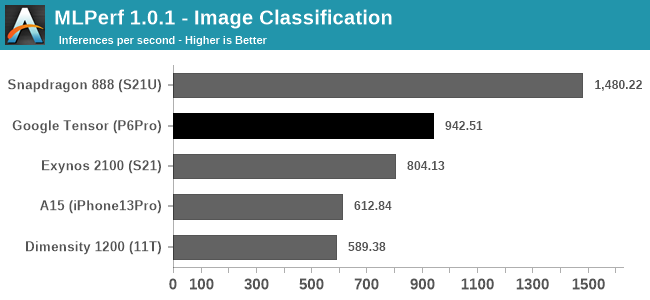
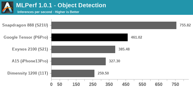
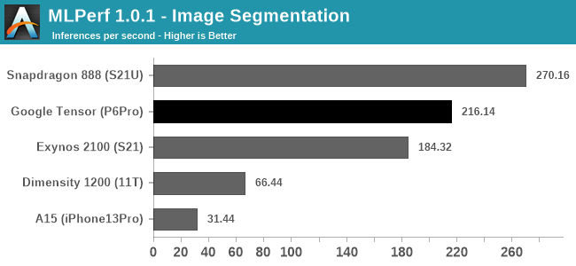
Starting off with the Image Classification, Object Detection, and Image Segmentation workloads, the Pixel 6 Pro and the Google Tensor showcase good performance, and the phone is able to outperform the Exynos 2100’s NPU and software stack. More recently, Qualcomm had optimised its software implementation for MLPerf 1.1, able to achieve higher scores than a few months ago, and this allows the Snapdragon 888 to achieve significantly better scores than what we’re seeing on the Google Tensor and the TPU – at least for those workloads, in the current software releases and optimisations.
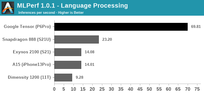
The Language Processing test of MLPerf is a MobileBERT model, and here for either architectural reasons of the TPU, or just a vastly superior software implementation, the Google Tensor is able to obliterate the competition in terms of inference speed.
In Google’s marketing, language processing, such as live transcribing, and live translations, are very major parts of the differentiating features that the new Google Tensor enables for the Pixel 6 series devices – in fact, when talking about the TPU performance, it’s exactly these workloads that the company highlights as being the killer use-cases and what the company calls state-of-the-art.
If the scores here are indeed a direct representation of Google’s design focus of the TPU, then that’s a massively impressive competitive advantage over other platforms, as it represents a giant leap in performance.
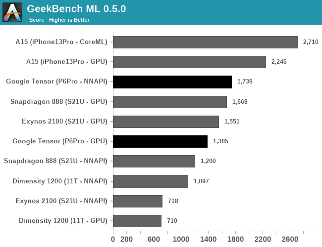
Other benchmarks we have available are for example GeekBench ML, which is currently still in a pre-release state in that the models and acceleration can still change in further updates.
The performance here depends on the APIs used, with the test either allowing TensorFlow delegates for the GPU or CPU, or using NNAPI on Android devices (and CoreML on iOS). The GPU results should only represent the GPU ML performance, which is surprisingly not that great on the Tensor, as it somehow lands below the Exynos 2100’s GPU.
In NNAPI mode, the Tensor is able to more clearly distinguish itself from the other SoCs, showcasing a 44% lead over the Snapdragon 888. It’s likely this represent the TPU performance lead, however it’s very hard to come to conclusions when it comes to such abstractions layer APIs.
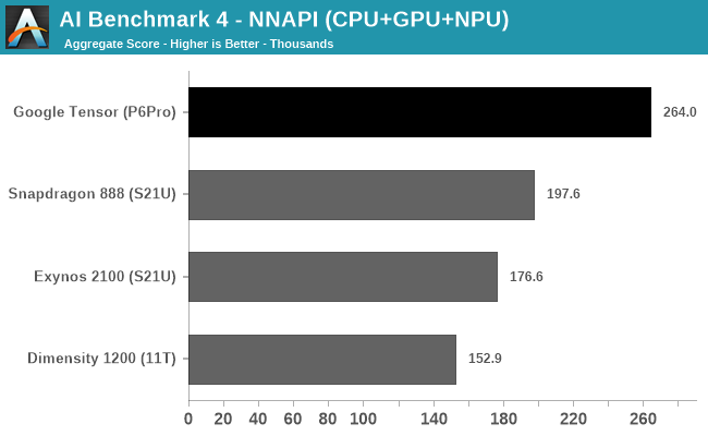
In AI Benchmark 4, when running the benchmark in pure NNAPI mode, the Google Tensor again showcases a very large performance advantage over the competition. Again, it’s hard to come to conclusions as to what’s driving the performance here as there’s use of CPU, GPU, and NPUs.
I briefly looked at the power profile of the Pixel 6 Pro when running the test, and it showcased similar power figures to the Exynos 2100, which extremely high burst power figures of up to 14W when doing individual inferences. Due to the much higher performance the Tensor showcases, it also means it’s that much more efficient. The Snapdragon 888 peaked around 12W in the same workloads, so the efficiency gap here isn’t as large, however it’s still in favour of Google’s chip.
All in all, Google’s ML performance of the Tensor has been its main marketing point, and Google doesn’t disappoint in that regard, as the chip and the TPU seemingly are able to showcase extremely large performance advantages over the competition. While power is still very high, completing an inference faster means that energy efficiency is also much better.
I asked Google what their plans are in regards to the software side of things for the TPU – whether they’ll be releasing a public SDK for developers to tap into the TPU, or whether things will remain more NNAPI centric like how they are today on the Pixels. The company wouldn’t commit yet to any plans as it’s still very early – in generally that’s the same tone we’ve heard from other companies as even Samsung, even 2 years after the release of their first-gen NPU, doesn’t publicly make available their Eden SDK. Google notes that there is massive performance potential for the TPU and that the Pixel 6 phones are able to use them in first-party software, which enables the many ML features for the camera, and many translation features on the phone.


108 Comments
View All Comments
anonym - Sunday, November 7, 2021 - link
I don't have any data but A76 is more efficient than A78 while relatively lower performance region. According to following DVFS carves, A77 is out of the question.https://images.anandtech.com/doci/15813/A78-X1-cro...
boozed - Tuesday, November 2, 2021 - link
So do we call this design "semi-custom" or "very-slightly-custom"?watzupken - Wednesday, November 3, 2021 - link
I think we have come to a point that pushing performance for mobile devices is starting to slow down big time, or in some cases like Exynos where we see regressions. The SOC gets refreshed each year, pushing for higher performance. The fabs however is slower to catch up, and despite the marketing of 7nm, 5nm, 3nm, etc, they may not be anywhere near what is being marketed. In this case, squeezing a fat GPU sounds great on paper, but in real life, the sustained performance is not going to make a huge difference because of the power and heat. In any case, I feel the push for an annual SOC upgrade should slow down because I certainly don't see significant difference in real life performance. We generally only know that last years SOCs are slower only when running benchmarks. Even in games, last gen high end SOCs can still handle challenging titles. Instead, they should focus on making the SOCs more power efficient.damianrobertjones - Wednesday, November 3, 2021 - link
All I want is for all phones to be able to record the front and rear camera at the same time. VLog fun. Such a simple thing... .Whiteknight2020 - Wednesday, November 3, 2021 - link
Not India, China, UK, Russia, most of the EU, Africa. Which is the vast majority of the world's population and the vast majority of the world's phones, a great many of which are still feature phones.Whiteknight2020 - Wednesday, November 3, 2021 - link
Not India, China, UK, Russia, most of the EU, Africa. Which is the vast majority of the world's population and the vast majority of the world's phones, a great many of which are still feature phones.eastcoast_pete - Wednesday, November 3, 2021 - link
To me, one of the most interesting points about this "meh" first Google custom SoC is that it was created with lots of Lego blocks from Samsung; I guess Google working with Qualcomm was either out of the question or not something either was willing to do. Maybe this was about Google wanting to show QC that they can develop a Pixel smartphone without them, maybe the two compete too closely on ML/AI, or maybe they just don't like each other much right now - who knows? Still, an SD 888-derived SoC with Google TPU would have likely been better on performance and efficiency. This one here is an odd duck. As for the Pixel 6, especially the Pro: camera is supposed to be spectacular, but with the battery life as it is and, of course (Google, after all), no expandable storage and no 3.5 mm headphone connectors, it missed the mark for me. But, the Pixels are sold out, so why would Google change?Whiteknight2020 - Wednesday, November 3, 2021 - link
If you want a "really excellent camera", sorry to disappoint you but you'll need to be buying an actual camera. The only thing a multipurpose portable computing device can ever be excellent at is being a multipurpose portable computing device.FunBunny2 - Wednesday, November 3, 2021 - link
"a multipurpose portable computing device."isn't that pretty much verbatim what Stevie said when he showed the original iPhone? nothing has really changed since. it was, kinda, a big deal when Stevie intoned that the thingee incorporated 3, count em 3!, devices that you had to carry that day!!! internet, phone, and number 3 (whatever that was). is a 2021 smartphone really anything more?? I mean, beyond the capacity of more transistors. thank ASML (and some really smart physicists and engineers) for that not Apple or Samsung or Google or ... last time I checked Apple's 'our own ARM' SoC is just bigger and wider ARM ISA, due to the, so far, increasing transistor budget available at the foundries.
that all begs the fundamental question: if Apple and The Seven Dwarfs have access to the same physical capital (ASML, et al) why the difference? if everybody spends time and money tweaking a function (that they all need, one way or another), in some time (short, I'll assert) The One Best Way emerges. the task, in the final analysis, is just maths. of course, Best is not a point estimate, as many comments make clear; there're trade offs all along the line.
it would be fun to use one of the Damn Gummint's supercomputers (weather or nucular bomb design) to spec a SoC. wonder how different the result would be?
NaturalViolence - Wednesday, November 3, 2021 - link
The math for the memory bandwidth doesn't check out. From the article:"4x 16-bit CH
@ 3200MHz LPDDR5 / 51.2GB/s"
But 3200MHz x 64 bit is 25.6GB/s, not 51.2GB/s. So which is it?