Google's Tensor inside of Pixel 6, Pixel 6 Pro: A Look into Performance & Efficiency
by Andrei Frumusanu on November 2, 2021 8:00 AM EST- Posted in
- Mobile
- Smartphones
- SoCs
- Pixel 6
- Pixel 6 Pro
- Google Tensor
Memory Subsystem & Latency
Usually, the first concern of a SoC design, is that it requires that it performs well in terms of its data fabric and properly giving its IP blocks access to the caches and DRAM of the system within good latency metrics, as latency, especially on the CPU side, is directly proportional to the end-result performance under many workloads.
The Google Tensor, is both similar, but different to the Exynos chips in this regard. Google does however fundamentally change how the internal fabric of the chip is set up in terms of various buses and interconnects, so we do expect some differences.
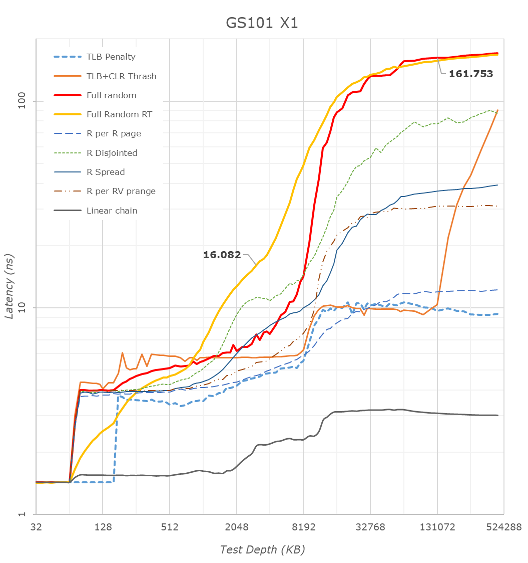
First off, we have to mention that many of the latency patterns here are still quite a broken due to the new Arm temporal prefetchers that were introduced with the Cortex-X1 and A78 series CPUs – please just pay attention to the orange “Full Random RT” curve which bypasses these.
There’s a couple of things to see here, let’s start at the CPU side, where we see the X1 cores of the Tensor chip being configured with 1MB of L2, which comes in contrast with the smaller 512KB of the Exynos 2100, but in line with what we see on the Snapdragon 888.
The second thing to note, is that it looks like the Tensor’s DRAM latency isn’t good, and showcases a considerable regression compared to the Exynos 2100, which in turn was quite worse off than the Snapdragon 888. While the measurements are correct in what they’re measuring, the problem is a bit more complex in the way that Google is operating the memory controllers on the Google Tensor. For the CPUs, Google is tying the MCs and DRAM speed based on performance counters of the CPUs and the actual workload IPC as well as memory stall % of the cores, which is different to the way Samsung runs things which are more transactional utilisation rate of the memory controllers. I’m not sure of the high memory latency figures of the CPUs are caused by this, or rather by simply having a higher latency fabric within the SoC as I wasn’t able to confirm the runtime operational frequencies of the memory during the tests on this unrooted device. However, it’s a topic which we’ll see brought up a few more times in the next few pages, especially on the CPU performance evaluation of things.
The Cortex-A76 view of things looks more normal in terms of latencies as things don’t get impacted by the temporal prefetchers, still, the latencies here are significantly higher than on competitor SoCs, on all patterns.
What I found weird, was that the L3 latencies of the Tensor SoC also look to be quite high, above that of the Exynos 2100 and Snapdragon 888 by quite a noticeable margin. I noted that one weird thing about the Tensor SoC, is that Google didn’t give the DSU and the L3 cache of the CPU cluster a dedicated clock plane, rather tying it to the frequency of the Cortex-A55 cores. The odd thing here is that, even if the X1 or A76 cores are under full load, the A55 cores as well as the L3 are still running at lower frequencies. The same scenario on the Exynos or Snapdragon chip would raise the frequency of the L3. This behaviour and aspect of the chip can be confirmed by running at dummy load on the Cortex-A55 cores in order to drive the L3 higher, which improves the figures on both the X1 and A76 cores.
The system level cache is visible in the latency hump starting at around 11-13MB (1MB L2 + 4MB L3 + 8MB SLC). I’m not showing it in the graphs here, but memory bandwidth on normal accesses on the Google chip is also slower than on the Exynos, but I think I do see more fabric bandwidth when doing things such as modifying individual cache lines – one of the reasons I think the SLC architecture is different than what’s on the Exynos 2100.
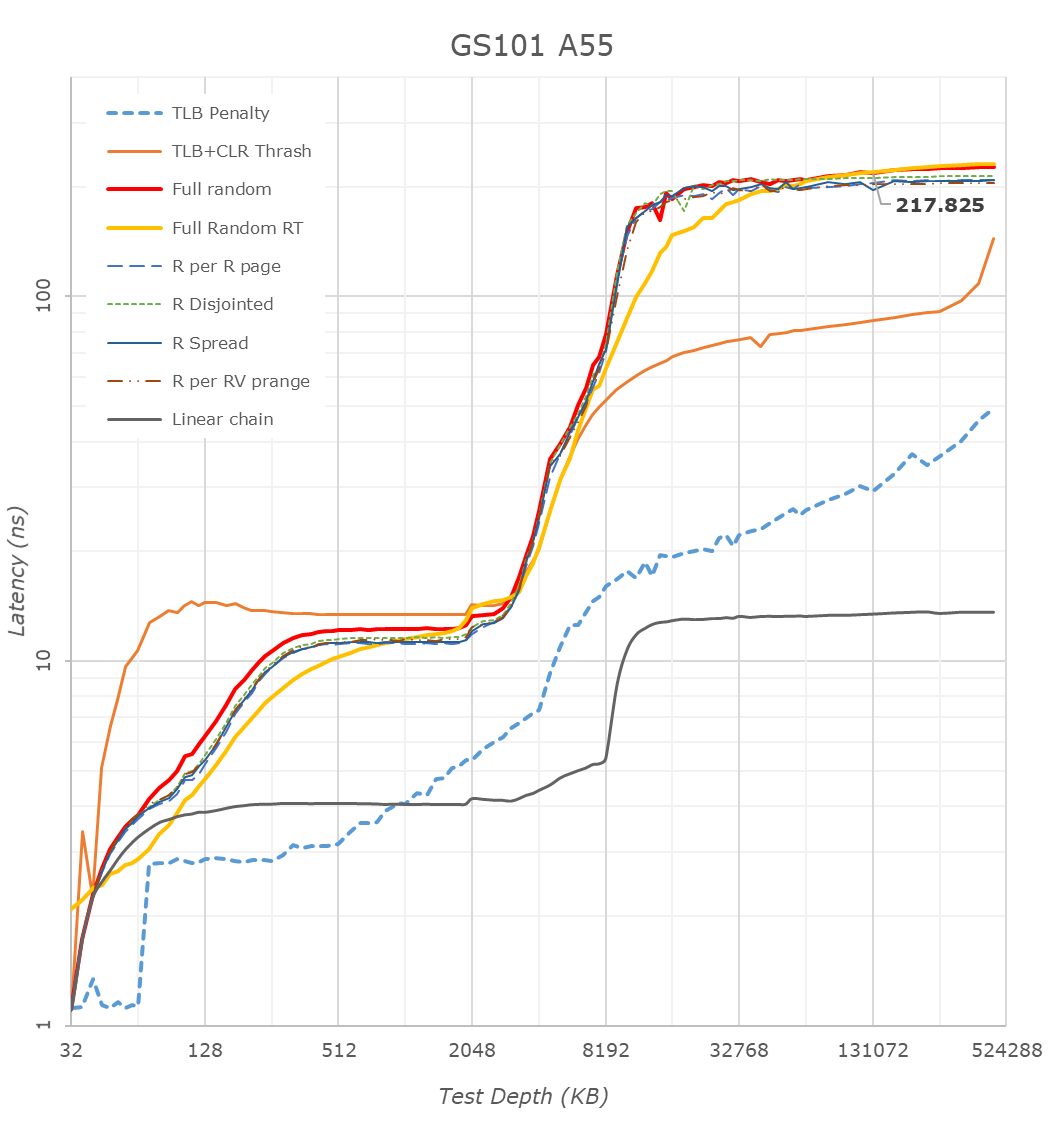
The A55 cores on the Google Tensor have 128KB of L2 cache. What’s interesting here is that because the L3 is on the same clock plane as the Cortex-A55 cores, and it runs at the same higher frequencies, is that the Tensor’s A55s have the lowest L3 latencies of the all the SoCs, as they do without an asynchronous clock bridge between the blocks. Like on the Exynos, there’s some sort of increase at 2MB, something we don’t see on the Snapdragon 888, and I think is related to how the L3 is implemented on the chips.
Overall, the Tensor SoC is quite different here in how it’s operated, and there’s some key behaviours that we’ll have to keep in mind for the performance evaluation part.


108 Comments
View All Comments
Alistair - Wednesday, November 3, 2021 - link
It's the opposite, the iPhone is massively ahead in performance, but every high end phone takes the same high end photos... you got the same photos but a lot less performance...aclos3 - Saturday, November 6, 2021 - link
I took some time to really test the camera and you are simply wrong. I have been photographing with it heavily for the last couple of days and the camera is incredible. Call it a gimmick or whatever, but the way they do their photo stacking puts this phone in a league of its own. If your main use case for a phone is benchmarking, I guess this is not your device.Lavkesh - Thursday, November 11, 2021 - link
Everyone and their grand mother do image stacking. iPhone is almost as good if not better even with a smaller sensor when compared to the latest Pixel. How's that for "in a league of its own"?Amandtec - Wednesday, November 3, 2021 - link
I don't doubt the veracity of your comment but I find the hostile undertone somewhat curious.damianrobertjones - Wednesday, November 3, 2021 - link
But... but... they said that it's amazing!! Who do I believe? /sZoolook - Saturday, November 6, 2021 - link
As long as they use Samsung process they will be hopelessly behind Apples Socs in efficiency unfortunately, would be interesting to see SD back on TSMC process for a direct comparison with Apple silicon.Tigran - Tuesday, November 2, 2021 - link
Performance looks very disappointing. Google promised 4.7x GPU performance improvement vs Pixel 5.singular9 - Tuesday, November 2, 2021 - link
I was enjoying how the speculation about the GS101 were claiming its "not far behind" the SD888. I was never expecting google to make another high end device, let alone one that undercuts most of the competition, as its just not what trends would say.I am not impressed. As someone who was rather hopeful that google would take control and bring us android users a true apple chip equivalent some day, this is definitely not the case with google silicon.
Considering how cookie cutter this design is, and how google made some major amateur decisions, I do not see google breaking away from the typical android SOC mold next generation.
Looking back at how long it took apple to design a near 100% solo design for the iPhone (A8X was the first A chip to use a complete inhouse GPU and etc design, other than ARM cores), that is a whopping 4 and a half years. Suppose this first google "designed" chip is following the same trend, an initial "brand name" break away yet still using a lot of help from other designs, and then slowly fixing one part at a time till its all fixed, while also improving what is already good, I could see google getting there by the Pixel X (10?). But as it stands, unless google dedicates a lot of time to actually altering Arm's own designs and simply having samsung make it, I don't see Tensor every surpassing qualcomm (unless samsung has some big breakthrough in their own CPU/GPU IP which may or may not come with AMD's help).
As the chip stands today, its "passable", but not impressive. Considering Google can get android to run really well on a SD765G, this isn't at all surprising. The TPU seems like a nice touch, since honestly, focusing on voice is more important than on "raw" cpu performance or something. I have always been frustrated with speech to text not being "perfect" and constantly having to correct it manually and "working around" its limitations. As for my own experience with the 6 Pro, its bloody good.
Now to specifics.
The X1 chips do get hot, as does the 5G modem. I switched the device to LTE for now. I do get 5G at home and pretty much most places I go, and it is fast, its not something I need right now. I even had a call drop over 5G because I walked around a buildings corner. Not fun.
The A76 excuse I have heard floating around, is that it takes up less physical die space, by A LOT. And apparently, there was simply no room for an A77 or A78 because the TPU and GPU took up so much room. I don't understand this compromise, when the GPU performance is this mediocre. Why not simply use the same GPU size as the S21 (Ex2100) and give the A78's more room? Don't know, but an odd choice for sure.
The A55 efficiency issues are noticeable. Try playing spotify over bluetooth for an hour, and watch the battery drain. I get consistently great standby time, and very good battery life when heavily using my device, but its these background screen off tasks that really chug the battery more than expected.
Over all though I haven't noticed any serious issues with my unit. The finger print scanner works as intended, and is better than my 8T. The camera does just as well if not better than the previous pixels. And over all...no complaints. But I wonder how much of this UX comes from google literally brute forcing their way with 2 X1 cores and a overkill GPU, and how much of it is them actually trying.
As for recommendations to google for Tensor V2, they need to not compromise efficiency for performance. This phone isn't designed to game, cut the GPU down, or heck, partner with AMD (who is working with samsung) to bring competitive graphics to mobile to compete with Adreno from QComm. 2 X1 cores, if necessary, can stay, but at that point, might as well just have 4 of them and get rid of all the other cores entirely and simply build a very good kernel to modulate the frequency. Or make it a 2+6 design with A57 cores. As someone who codes kernels for pixels and nexus devices for a long time, trying to optimize the software to really get efficiency out of the big.LITTLE system is near impossible, and in my opinion, worthless unless your entire scheduler is "screen on/off" based, which is literally BS. I doubt google has any idea how to build a good CPU governor nor scheduler to truly make this X+X+X system even work properly, since I have yet see qcomm or samsung do it "well" to call commendable.
The rest of the phone is fine. YoY improvements are always welcome, but I think the pixel 6/pro just really show how current mobile chips are so far behind apple that you might as well give up. YoY improvements have imo halted, and honestly no one seems to be having the thought that maybe we should cut power consumption in half WITHOUT increasing performance. I mean...the phones are fast enough.
Who knows. We will see next year.
PS: I also am curious what google will do with the Pixel 6A (if they make one at all). Will it use a cut down GS101 or will it get the whole chip? It would seem overkill to shove this into a 399$ phone. Wonder what cut downs will be made, or if there will be improvements as well.
sharath.naik - Tuesday, November 2, 2021 - link
Good thoughts, there is one big issue you missed. Pixel camera sensors 50mp/48mp being binned to 12mp yet Google labeled them as 50mp/48mp. Every shot outside the native 1x,4x is just a crop of the 12mp image including pottaitk3mp crop) and 10x(2.5mp crop}.teldar - Thursday, November 4, 2021 - link
You are absolutely a clueless troll and should go back to your cave. Your stupidity is unwanted.