Intel 4 Process Node In Detail: 2x Density Scaling, 20% Improved Performance
by Ryan Smith on June 13, 2022 7:00 AM EST
Taking place this week is the IEEE’s annual VLSI Symposium, one of the industry’s major events for disclosing and discussing new chip manufacturing techniques. One of the most anticipated presentations scheduled this year is from Intel, who is at the show to outline the physical and performance characteristics of their upcoming Intel 4 process, which will be used for products set to be released in 2023. The development of the Intel 4 process represents a critical milestone for Intel, as it’s the first Intel process to incorporate EUV, and it’s the first process to move past their troubled 10nm node – making it Intel’s first chance to get back on track to re-attaining fab supremacy.
Intel’s scheduled to deliver their Intel 4 presentation on Tuesday, in a talk/paper entitled “Intel 4 CMOS Technology Featuring Advanced FinFET Transistors optimized for High Density and High-Performance Computing”. But this morning, ahead of the show, they re publishing the paper and all of its relevant figures, giving us our first look at what kind of geometries Intel is attaining, as well as some more information about the materials being used.
Previously known as Intel’s 7nm process, Intel 4 is Intel’s first time using EUV lithography for their chips. A long time coming, the use of EUV promises both to allow Intel to draw the kind of ever-smaller features needed for more advanced manufacturing nodes, while at the same time letting Intel cut down on the number of manufacturing steps required via today’s multi-patterning DUV techniques. Unusually, Intel finds itself as the final of the big three fabs to tap into EUV – the company passed on EUV for the 10nm generation as they didn’t feel it was ready, and then delays with 10nm and 7nm pushed back Intel’s EUV adoption point significantly. As a result, Intel will get to spring forward on the basis of EUV-driven gains, though they will still have to make up for lost time and TSMC’s experience advantage.
The development of Intel 4 is also a critical juncture for the company, as it finally allows them to move past their troubled 10nm process. While Intel has managed to make something suitable of their 10nm process nodes – especially with their most recent 10nm Enhanced SuperFin variant, which we better know as Intel 7 – it’s not been without entirely too much blood, sweat, and years. Intel believes they tried to do too much all at once with 10nm – both in regards to scaling and in too many new manufacturing techniques – which in turn set them back years as they untangled that mess to find and iterate on what went wrong. Unsurprisingly then, Intel is being a bit less aggressive with their first EUV node, and the company overall has taken a much more modular development approach going forward, allowing for new technologies to be implemented (and, if necessary, debugged) in steps.
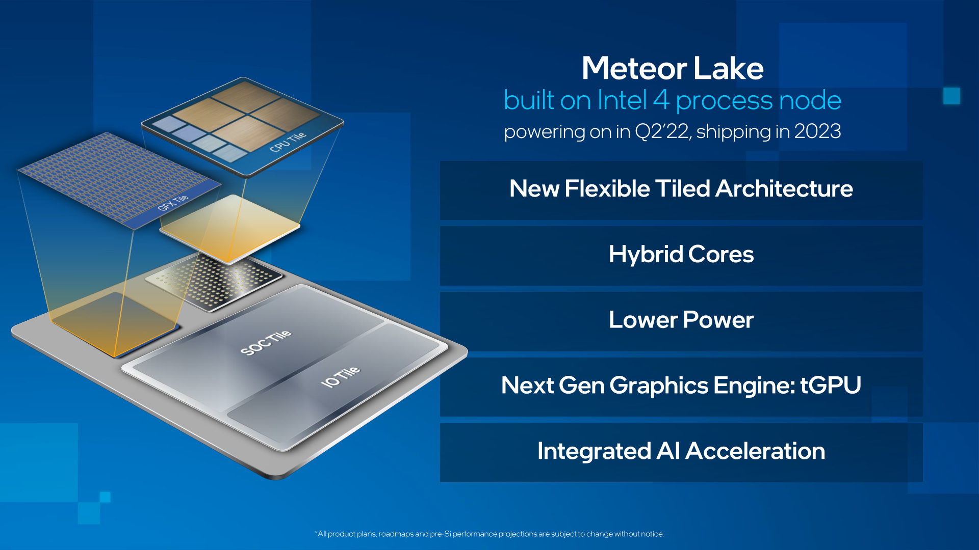
Intel 4, in turn, will be first used for Intel’s forthcoming Meteor Lake client SoC, which is expected to be the basis of Intel’s 14th generation Core processor family. Though not shipping until 2023, Intel already has Meteor Lake up and running in their labs, as per the company’s typical bring-up process. Along with brining a significant bump in process technologies, Meteor Lake will also be Intel’s first tiled/chiplet-based client CPU, using a mix of tiles for I/O, CPU cores, and GPU cores.
Intel 4 Physical Parameters: 2x Density Over Intel 7, Cobalt Use Continues
Diving into the Intel 4 process, Intel has set out to tackle a few different things here. First and foremost is, of course, density. Intel is striving to keep Moore’s Law alive, and while the coinciding death of Dennard scaling means that it’s no longer a simple matter of lighting up twice as many transistors on every generation, a higher transistor density affords smaller chips at with the same hardware, or throwing in more cores (or other processing hardware) with newer desgins.
| Comparing Intel 4 to Intel 7 | |||
| Intel 4 | Intel 7 | Change | |
| Fin Pitch | 30 nm | 34 nm | 0.88 x |
| Contact Gate Poly Pitch | 50 nm | 54/60 nm | 0.83 x |
| Minimum Metal Pitch (M0) | 30 nm | 40 nm | 0.75 x |
| HP Library Height | 240h | 408h | 0.59 x |
| Area (Library Height x CPP) | 12K nm2 | 24.4K nm2 | 0.49 x |
Of the figures Intel is releasing in this week’s paper, the fin pitch on Intel 4 is down to 30nm, 0.88x the size of Intel 7’s 34nm pitch. Similarly, the pitch between contact gates is now 50nm, down from 60nm before. But most significantly, the minimum metal pitch for the lowest layer (M0) is also 30nm, 0.75x the size of the M0 pitch on Intel 7.
Intel’s library height has also been cut down as well. The cell height for the high-performance library on Intel 4 is 240nm, which is only 0.59 x the height of an HP cell on Intel 7.
As a result, Intel is claiming a 2x increase in density for Intel 4 versus Intel 7 – or more specifically, a halving of size for transistors – a traditional, full node’s improvement in transistor density.
Since chips are 2D constructs, the metric Intel uses for this is multiplying the HP cell height by the contacted poly pitch, which is essentially the width of a cell. In that case they get 24,408 nm2 for Intel 7, and a flat 12,000 nm2 for Intel 4, 0.49x the area of the Intel 7-based cell.
Of course, not every type of structure scales by the same factor with a new process node, and Intel 4 is no different. According to the company SRAM cells on Intel 4 are only around 0.77x the size of the same cells on Intel 7. So while standardized logic cells have doubled in density, SRAM density (for equivalent SRAM types) has only improved by 30% or so.
And, unfortunately, while Intel is talking about density with respect to standard cells, they aren’t officially disclosing actual transistor density figures. For now, what Intel is telling us is that the overall transistor density translates well with the 2x figure they’re currently providing. Which, based on what we know about Intel 7 and its 80 million transistors per mm2 density for HP libraries, would place Intel 4's HP libraries at around 160MTr/mm2.
Since these figures are for Intel's lower density high-performance libraries, the obvious follow-up question to that would be what the figures are for high density libraries – which traditionally squeeze things even more in exchange for reduced clockspeeds. However as it turns out, Intel won’t be developing high density libraries for Intel 4. Instead, Intel 4 will be a pure high-performance node, and high-density designs will come with the successive node, Intel 3.
This unusual development comes as a result of Intel’s modularization efforts for process node development. Intel has essentially adopted a tick tock-like strategy for node development over the next half decade or so, with Intel developing an initial node based on a new technology (e.g. EUV or High-NA machines), and then following that up with a more refined/optimized successor. In the case of Intel 4, while it’s doing important pioneering work for EUV within Intel’s fabs, the company’s bigger plans are for Intel 3 to be their long-term, long-lived EUV node.
All of which means that Intel has no need for high-density libraries with Intel 4, since it is slated to be replaced with the more fully-featured Intel 3 within a year or so. And since Intel 3 is design compatible with Intel 4, it’s clear to see how Intel is pushing its own design teams to use the latter process whenever timetables allow. Intel Foundry Services customers will also be a in a similar boat – they can use Intel 4, but IFS is more focused on supplying access to and design help with Intel 3.
Getting back to Intel 4 itself, the new node comes with a significant change to the metal layers as compared to Intel’s 10nm processes. Intel famously replaced copper with cobalt at the lowest layers of its 10nm process, something that the company deemed necessary for transistor longevity (electromigration resistance) reasons. Unfortunately, cobalt isn’t as good from a performance (clockspeed) perspective, and it’s long been suspected that the switch to cobalt was one of the major stumbling blocks in 10nm development for Intel.
For Intel 4, in turn, Intel is taking half a step back. The company is still using cobalt in their processes, but now rather than pure cobalt they are using what they are calling Enhanced Copper (eCu), which is copper cladded with cobalt. The idea behind eCu is to have the best of both words, maintaining the performance of a doped copper metallization layer, while still getting the electromigration resistance benefits of cobalt.
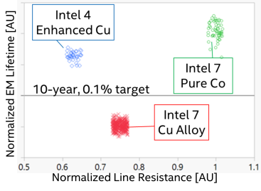
Electromigration lifetimes and line Resistance are compared for different metallurgy options.
And while Intel is no longer using pure cobalt, in some respects their use of cobalt is increasing overall. Whereas Intel’s 10nm processes only used cobalt for the contact gate and first two metal layers, Intel 4 is expanding the use of eCu to the first 5 metal layers. As a result, the lowest-third of the complete metal layer stack in a chip is using Intel’s cobalt-clad copper. Intel has, however, removed cobalt from the gate itself; that’s now pure tungsten, rather than a mix of tungsten and cobalt.
| Intel 4 Metal Stack | ||
| Layer | Metal | Pitch |
| Fin | - | 30 nm |
| Gate | Tungsten | 50 nm |
| Metal 0 | Copper w/Cobalt Cladding | 30 nm |
| Metal 1 | Copper w/Cobalt Cladding | 50 nm |
| Metal 2 | Copper w/Cobalt Cladding | 45 nm |
| Metal 3 | Copper w/Cobalt Cladding | 50 nm |
| Metal 4 | Copper w/Cobalt Cladding | 45 nm |
| Metal 5, 6 | Copper | 60 nm |
| Metal 7, 8 | Copper | 84 nm |
| Metal 9, 10 | Copper | 98 nm |
| Metal 11, 12 | Copper | 130 nm |
| Metal 13, 14 | Copper | 160 nm |
| Metal 15 | Copper | 280 nm |
| Giant Metal 0 | Copper | 1080 nm |
| Giant Metal 1 | Copper | 4000 nm |
All told, the number of metal layers for Intel 4 has increased versus Intel 7. Whereas the latter had 15 metal layers for logic, Intel 4 squeezes in a 16th layer. This is joined by the usual two layers for power routing, which Intel terms its giant layers due to their relatively massive pitches of 1080nm and 4000nm.
Alongside the tighter gate and metal layer pitches, another area where Intel is gaining density improvements from design rule changes for interconnects. With Intel 4, Intel has moved to what they’re calling a gridded interconnect design, which in short, only allows for vias going between metal layers to be placed per a pre-determined grid. Previously, vias could be placed anywhere, which allowed for some flexibility, but had other trade-offs.
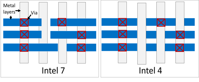
Design rules changed from traditional (left) to gridded (right) to improve yield and improve performance though capacitance reduction
According to Intel, the use of grids has improved both the yields of the process by reducing variability, as well as how they go about optimizing designs. The switch also has a side benefit of allowing Intel to avoid having to use complex, multi-patterned EUV for their interconnects.
Finally, as previously mentioned, the use of EUV is also allowing Intel to reduce the number of steps (and the number of masks) required to fab a chip. While the company isn’t offering absolute numbers, on a relative basis Intel 4 requires 20% fewer masks than Intel 7. Had Intel not done this, the number of masks required would have instead shot up by around 30% due to the number of multi-patterning steps required.
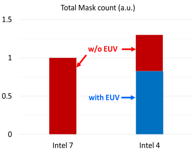
Extensive employment of EUV enables feature scaling and process simplification
The use of EUV is also having a positive impact on Intel’s yields. Though the company isn’t providing exact numbers, the reduction in the number of steps offers fewer opportunities for anything to go wrong that would introduce a defect on a wafer.
Intel 4 Performance: 21.5% More Perf at iso-power/40% Less Power at iso-frequency
Density improvements aside, what kind of performance improvements is Intel seeing for the Intel 4 process? In short, Intel is seeing above-average gains in both frequencies and power efficiency.
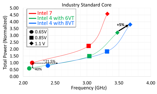
Circuit analysis of industry standard core shows 21.5% performance gain at matched power over Intel 7 at 0.65V. 8VT flow enables 5% performance gain over 6VT at high voltages.
At an iso-power of 0.65v, Intel is seeing a 21.5% increase in clockspeeds attainable versus Intel 7. With that said, 0.65v is at the low end of the curve, and Intel’s graph does show diminishing returns as you go farther up in voltage; at 0.85v and beyond the iso-power gains are closer to 10%. According to Intel, they can squeeze out another 5% or so by using cells designed for higher threshold voltages (8VT), which comes at a cost of higher total power consumption versus standard cells.
And if we take things from the other end, Intel is reporting even larger gains on the power efficiency front with Intel 4. At iso-frequency – in this case around 2.1GHz – Intel is seeing 40% lower power consumption. There are again diminishing returns as frequencies increase (up until Intel 7 hits its practical limits), but it’s more consistent than the performance/frequency gains. This mirrors what we’ve seen with other process nodes – including Intel 7 at its launch – where newer nodes are reducing power consumption at a much greater rate than they’re enabling higher clockspeeds. A full CPU built on the Intel 4 process could conceivably save a great deal of power – so long as you don’t mind it not clocking any higher than before.
All told, the performance gains outlined in Intel’s paper mirror those that they have been claiming up until now, such as the 20% perf-per-watt gains for Intel 4 discussed at last summer’s process roadmap update. For the last year Intel has been approaching the finishing line for Intel 4 development, so as their paper outlines, they appear to be on-track for delivering on their performance gains.
Meanwhile, Intel is also reporting good developments in cost scaling from Intel 7 to Intel 4, though once again the company isn’t providing specific numbers. 1 EUV layer does end up being more expensive than 1 DUV layer, but because EUV eliminates a bunch of multi-patterning, it helps to bring down the total costs by reducing the total number of steps. The switch to EUV is also reducing a bit of the capital pressure on Intel, as Intel 4 doesn’t require quite as much clean room space (though it’s by no means a small amount overall).
Ultimately, as Intel looks to ship Meteor Lake and other first-generation Intel 4 products in 2023, what remains to be seen is how quickly Intel can get their new process node up and running to the standards of high-volume manufacturing. With Meteor Lake samples already in Intel’s labs, Intel is getting ever closer to finally entering the EUV age. But for Intel, hitting all of their goals getting there means not just scaling up production from their Hillsboro development fab, but also mastering the interesting task of replicating their process to Ireland and the other Intel fabs that will be used for Intel 4.


129 Comments
View All Comments
JayNor - Monday, June 13, 2022 - link
Intel also has a presentation today on an Intel-4 RISC-V chip.C8-1: An 8-core RISC-V Processor with Compute near Last Level Cache in Intel 4 CMOS
JayNor - Monday, June 13, 2022 - link
another presentation Thursday on an SRAM design on Intel-4 process...C24-1 - Energy-Efficient High Bandwidth 6T SRAM Design on Intel 4 CMOS Technology
KPOM - Tuesday, June 14, 2022 - link
If Intel does pull even with TSMC at 20A or ahead at 18A, it will be interesting to see if Apple considers using Intel Fab Services for at least part of their production.Zoolook - Wednesday, June 15, 2022 - link
Historically they don't shift supplier that quickly when in an established partnership, only when a trend is established, so I'd guess you need to see TSMC faling behind until they would switch.SiliconFly - Friday, June 24, 2022 - link
Well, historically apple has always had more than one supplier for all their key components. But when it comes to fabs, they're stuck with tsmc for obvious reasons. No other fabs offer good nodes. Once Intel IFS opens gate with advanced nodes than tsmc, apple will sure grab a bite. It's in their DNA.Spunjji - Wednesday, June 15, 2022 - link
Overall this looks very positive for Intel, but as always, there's a couple of bits that make me chuckle when I read between the lines. For example:"In short, Intel is seeing above-average gains in both frequencies and power efficiency."
This is much easier to achieve when your previous process had below-average properties in these areas! Intel 7 was a huge improvement over the original 10nm, but 10nm may have been one of the worst manufacturing processes in recent memory, and 7 still shows some of its weaknesses, like the unreasonably large surge in power needed to hit competitive clock speeds.
Silver5urfer - Friday, June 17, 2022 - link
Intel is fixing their issues is what I can understand and the EUV process finally. Plus the best part is Clockspeed boost. However the worst part is bigLittle trash for Intel CPUs until 2025+ they retire the CORE series by then.The future is going to be uArch and Clockspeed. Intel's 7 / 10nm is already denser than TSMC N7, Intel 4 is going to compete with AMD's Zen 5 on N5 or N4 nodes at best. So it all boils to the uArch scalability. Since Zen 4 is showing 5.5GHz under the ADL PL2 I think AMD is winning the Arch design, Zen is a new uArch vs CORE.
Apple is irrelevant garbage because they do not compete in XEON and Mainstream LGA socket, they fight in the BGA land.
GeoffreyA - Friday, June 17, 2022 - link
To me it's all meaningless because soon there won't be any node improvements any more. The question is, how far can architecture go, and can there be some new development in computing?Silver5urfer - Friday, June 17, 2022 - link
Since it's more of an unknown I will go by my dystopian picture of it.2030 is where Great Reset is being planned so I'm assuming some massive changes in computing might occur at that point, give or take by 2035. But I believe that DIY PC will die eventually because of high cost in manufacturing and slowly market waning, looking at the volume of Smartphones and BGA Lapjokes that ship is very high in numbers people are fine with consuming use and throw junk more than anything, imagine an AirPods division is out pacing AMD, Nvidia and likes in sheer profits !! That's the level of consumerism you have right now. It's insane.
AR/VR/MR once Apple releases the product, Mainstream adoption will be very high, which will result on Stadia / XCloud type garbage taking over, once that is done PC will die because masses do not care about owning, or even buying a great piece of art (games which are free from political ideologies).
But yea silicon won't go away until 2040, I doubt that. The corporations who want extreme power will make it centralized computing like the top Japanese Sci-Fi ones like say - Ergo Proxy, Psycho-Pass etc. But with ofc worse idpol.
GeoffreyA - Friday, June 17, 2022 - link
Yes, the DIY PC is slowly dying, and consumerist mobile is taking over, if it hasn't already done so. Plus, I suppose with the Web 3.0, metaverse nonsense, there'll be an ever greater push towards AR, VR, whatever it's called these days.Concerning computing, while I grant that some new discovery could throw open the doors, I wouldn't be surprised there's some fundamental limit to computation---well, serial computation at any rate---and we're asymptotically approaching it. A bit like the speed of light. And, if the universe itself is being computed, our AMD and Intel CPUs will never run faster than that. Of course, science can open new doors and has done so before; it might be something that is inconceivable at present.