Intel's 50Gbps Silicon Photonics Link: The Future of Interfaces
by Brian Klug on July 30, 2010 6:49 AM EST- Posted in
- Trade Shows
- Intel
- Photonics
- Laser
On Tuesday, Intel demonstrated the world’s first practical data connection using silicon photonics - a 50 gigabit per second optical data connection built around an electrically pumped hybrid silicon laser. They achieved the 50 gigabit/s data rate by multiplexing 4 12.5 gigabit/s wavelengths into one fiber - wavelength division multiplexing. Intel dubbed its demo the “50G Silicon Photonics Link.”
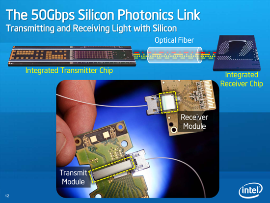
Fiber optic data transmission isn’t anything new - it’s the core of what makes the internet as we know it today possible. What makes Intel’s demonstration unique is that they’ve fabricated the laser primarily out of a low-cost, mass-produceable, highly understood material - silicon.
For years, chip designers and optical scientists alike have dreamt about the possibilities of merging traditional microelectronics and photonics. Superficially, one would expect it to be easy - after all, both fundamentally deal with electromagnetic waves, just at different frequencies (MHz and GHz for microelectronics, THz for optics).
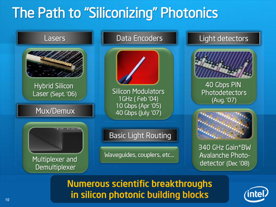
On one side, microelectronics deals with integrated circuits and components such as transistors, copper wires, and the massively understood and employed CMOS manufacturing process. It’s the backbone of microprocessors, and at the core of conventional computing today. Conversely, photonics employs - true to its name - photons, the basic unit of light. Silicon photonics is the use of optical systems that use silicon as the primary optical medium, instead of other more expensive optical materials. Eventually, photonics has the potential to supplant microelectronics with optical analogues of traditional electrical components - but that’s decades away.
Until recently, successfully integrating the two was a complex balance of manufacturing and leveraging photonics only when it was feasible. Material constraints have made photonics effective primarily as a long haul means of getting data from point to point. To a larger extent, this has made sense because copper traces on motherboards have been fast enough, but we’re getting closer and closer to the limit.


42 Comments
View All Comments
ghot - Thursday, August 5, 2010 - link
"Blinded by the light...." I'm 53 years old and having been waiting for this since the 1st TI calculator hit the market in 1976. Unfortunately I probably won't live to see the 1st totally optical, consumer affordable PC.This doesn't prove 'Murphy's Law....it squares or even cubes it.
The best part, isn't even the speed (although it will be incredible) but rather the fact that PCB printed circuits can be a long as the design requires. Imagine a motherboard 5 inches wide and 3-4 foot tall. Then a PC enclosure could look more like a 4 foot tall 6x6 inch speaker enclosure for example.
Cooling needs will be greatly reduced as well. Just try to imagine the over clocking potential.
I used to drool over the 1st commercially available digital watch...the Pulsar....didn't even have LED's...it used tiny Nixie Tubes.....and now this.
When most of you are my age, you'll be complaining that your brand new Intel P4 (yes P4..maybe in YOUR lifetime, Intel will get back to simple naming schemes) is only capable of 4Thz on air. And, as every over clocker knows....increase the speeds in small increments...say .....10Ghz each time...lol
I am so jealous :)
ziaullahk - Sunday, February 18, 2018 - link
And to think about it, we just reached 100GBps according to https://compoundtek.com/news