Everything You Always Wanted to Know About SDRAM (Memory): But Were Afraid to Ask
by Rajinder Gill on August 15, 2010 10:59 PM ESTSynchronous dynamic random access memory (SDRAM) is made up of multiple arrays of single-bit storage sites arranged in a two-dimensional lattice structure formed by the intersection of individual rows (Word Lines) and columns (Bit Lines). These grid-like structures, called banks, provide an expandable memory space allowing the host control process and other system components with direct access to main system memory to temporarily write and read data to and from a centralized storage location.
When associated in groups of two (DDR), four (DDR2) or eight (DDR3), these banks form the next higher logical unit, known as a rank. 2GB DDR3 Dual Inline Memory Modules (DIMM) are undoubtedly the most popular density choice among today's enthusiast users. Most new parts of this type are configured as two identical ranks of eight banks each; one side of the DIMM housing those ICs that make up Rank 1, with Rank 2 populating the opposite face of the module. For this reason, single-sided DIMMs typically comprise only a single rank of addressable memory space.
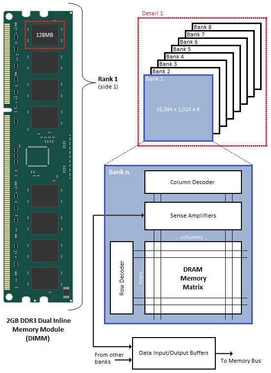
Figure 1 shows the typical functional arrangement of SDRAM memory space. In the case of our example dual-sided dual-rank unbuffered 2GB SDRAM DIMM, the fully populated module contains a total of 16 ICs, eight per side. Each IC contains eight banks of addressable memory space comprising 16K pages and 1K column address starting points with each column storing a single 8-bit word. This brings the total memory space to 128MB (16,384 rows/bank x 1,024 columns addresses/row x 1 byte/column address x 8 stacked banks) per IC. And since there are eight ICs per rank, Rank 1 is 1GB (128MB x 8 contiguous banks) in size, with the same for Rank 2, for a grand total of 2GB per module.
If each row contains 1K (1,024) column address staring points and each column stores 8 bits (1 byte), this would mean each row (page) is 8,192 bits (1,024 x 8 bits) or 1K bytes per bank. It's important to understand that each page of memory is segmented evenly across Bank n of each IC for the associated rank. For this reason, each page is in actuality 8KB (1KB x 8 contiguous banks) in size. So when we talk about IC density we are referring to eight distinct stacked banks and the total memory space therein, whereas when we talk about page space, we are really working with Bank n spread across the total number of ICs per rank. In the end the math comes out the same (8 ICs versus 8 banks), but conceptually it's a critical distinction worth acknowledging if we are to really grasp the ins and outs of memory addressing.
We can now see why the DDR3 core has a 8n-prefetch (where n refers to the number of banks per rank) as every read access to the memory requires a minimum of 64 bits (8 bytes) of data to be transferred. This is because each bank, of which there are eight for DDR3, fetches no less than 8 bits (1 byte) of data per read request - the equivalent of one column's worth of data. Whether or not the system actually makes use of all 8 bytes of transferred data is irrelevant. Any delivered data not actually requested can be safely disregarded as it's just a copy of what is still retained in memory.


46 Comments
View All Comments
JarredWalton - Monday, August 16, 2010 - link
Oh, it's missing a lot more than just voltage information. :-) There are rebates on most memory kits right now, for instance. Still, I felt it was useful to highlight where the current "best deals" tend to fall.I personally wouldn't touch the ultra-expensive $150+ stuff, but up to $115 has potential at least. For a lower voltage kit, G.Skill has an ECO line rated at DDR3-1600 7-8-7-24-2N and 1.35V for $103. Worth a look at least....
JarredWalton - Monday, August 16, 2010 - link
Note: I screwed up my table above. DDR3 is two bits per clock, so the base clocks are all twice what I listed, which means latency for CAS is half what I listed. Sorry. Got things confused with GDDR5. :-) The relative latency is still the same, of course, which is the main point.JarredWalton - Monday, August 16, 2010 - link
Side note number two: And of course, CAS Latency isn't the be-all, end-all. According to benchmarks by Raja, DDR3-2000 at 6-9-6 timings often trails RAM at 7-8-7, as the tRCD difference becomes more pronounced in some cases.Rajinder Gill - Monday, August 16, 2010 - link
Sorry I should have said 7-7-8 vs 6-9-8. This happens when the number of random access requests are high (fewer back to back reads). Benchmarks like WinRar and Super Pi (synthetic) are mainly the ones that show this.-Raja
Drag0nFire - Friday, August 20, 2010 - link
I've had great experience with the ECO line. Put the 2x2 kit you mentioned in two computers so far, and it's been great. Feels like a steal to get such high speed and low voltage at such a great price.kalniel - Monday, August 16, 2010 - link
Thanks for taking the time to write the article - the cycle time-line figures are very helpful, but I'm struggling to understand it correctly.Take fig. 5. There doesn't seem to be a Read to Precharge Delay. If we follow the recommendation of CL+tBurst = tRCP + tRP then won't there be a delay of 4T after the Data Read Burst before the RAS Precharge starts, giving a Row Cycle Time of 26 rather than 24?
kjboughton - Monday, August 16, 2010 - link
tRTP may very well be 4T but the minimum RAS Active Time (tRAS) is 18T. The precharge is precluded from occuring until this period has expired making the clock at T + 18 the first opportunity to precharge the bank. Add to this the RAS Precharge (tRP) and you have the Row Cycle Time (tRC = tRAS + tRP) - the minimum time any single row MUST remain open before it can be closed (and before another page in the same bank can be accessed).Does this help?
kalniel - Monday, August 16, 2010 - link
I thought the Read to Precharge Delay was there precisely to ensure you waited the minimum RAS active time before precharging the bank. Are you saying that the tRTP doesn't apply if you've already finished tRCD+CL+tBurst within tRAS so can start precharging as soon as minimum RAS active time is achieved?In other words, tRTP doesn't have a bearing on a single burst per page, but is there to help synchronise auto-precharge reads within the same page?
My ignorance may be beyond redemption!
kjboughton - Monday, August 16, 2010 - link
Read to Precharge Delay (tRTP) is the minimum wait time from a READ (column access) to bank PRECHARGE.RAS Active Time (tRAS) is the minimum wait time from an ACTIVATE (row access) to bank PRECHARGE.
Both times must be satisfied before the bank can be precharged. Perhaps I wasn't quite clear enough on this point. I hope this clears things up.
kalniel - Monday, August 16, 2010 - link
I think I've got it now, thanks. My brain saw the relevant diagram and screamed 'Cthulu' instead.