Everything You Always Wanted to Know About SDRAM (Memory): But Were Afraid to Ask
by Rajinder Gill on August 15, 2010 10:59 PM ESTSynchronous dynamic random access memory (SDRAM) is made up of multiple arrays of single-bit storage sites arranged in a two-dimensional lattice structure formed by the intersection of individual rows (Word Lines) and columns (Bit Lines). These grid-like structures, called banks, provide an expandable memory space allowing the host control process and other system components with direct access to main system memory to temporarily write and read data to and from a centralized storage location.
When associated in groups of two (DDR), four (DDR2) or eight (DDR3), these banks form the next higher logical unit, known as a rank. 2GB DDR3 Dual Inline Memory Modules (DIMM) are undoubtedly the most popular density choice among today's enthusiast users. Most new parts of this type are configured as two identical ranks of eight banks each; one side of the DIMM housing those ICs that make up Rank 1, with Rank 2 populating the opposite face of the module. For this reason, single-sided DIMMs typically comprise only a single rank of addressable memory space.
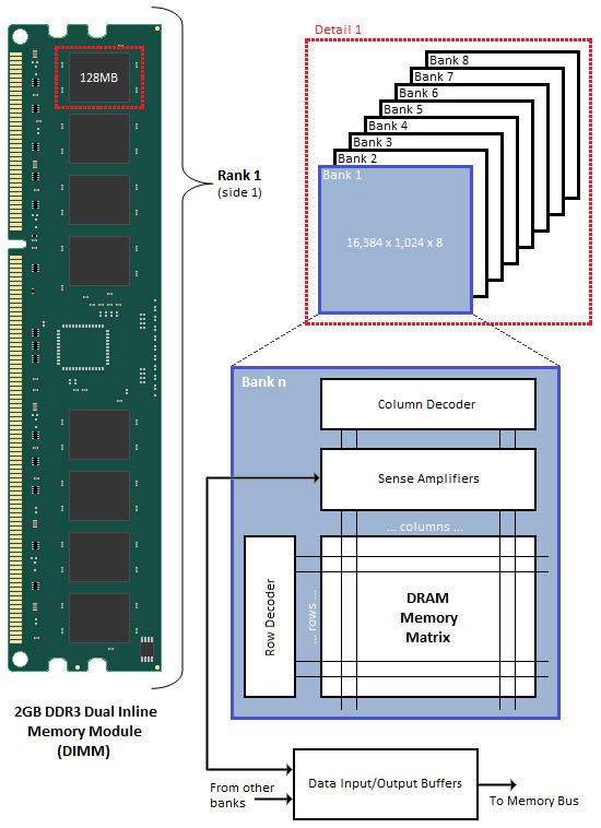
Figure 1 shows the typical functional arrangement of SDRAM memory space. In the case of our example dual-sided dual-rank unbuffered 2GB SDRAM DIMM, the fully populated module contains a total of 16 ICs, eight per side. Each IC contains eight banks of addressable memory space comprising 16K pages and 1K column address starting points with each column storing a single 8-bit word. This brings the total memory space to 128MB (16,384 rows/bank x 1,024 columns addresses/row x 1 byte/column address x 8 stacked banks) per IC. And since there are eight ICs per rank, Rank 1 is 1GB (128MB x 8 contiguous banks) in size, with the same for Rank 2, for a grand total of 2GB per module.
If each row contains 1K (1,024) column address staring points and each column stores 8 bits (1 byte), this would mean each row (page) is 8,192 bits (1,024 x 8 bits) or 1K bytes per bank. It's important to understand that each page of memory is segmented evenly across Bank n of each IC for the associated rank. For this reason, each page is in actuality 8KB (1KB x 8 contiguous banks) in size. So when we talk about IC density we are referring to eight distinct stacked banks and the total memory space therein, whereas when we talk about page space, we are really working with Bank n spread across the total number of ICs per rank. In the end the math comes out the same (8 ICs versus 8 banks), but conceptually it's a critical distinction worth acknowledging if we are to really grasp the ins and outs of memory addressing.
We can now see why the DDR3 core has a 8n-prefetch (where n refers to the number of banks per rank) as every read access to the memory requires a minimum of 64 bits (8 bytes) of data to be transferred. This is because each bank, of which there are eight for DDR3, fetches no less than 8 bits (1 byte) of data per read request - the equivalent of one column's worth of data. Whether or not the system actually makes use of all 8 bytes of transferred data is irrelevant. Any delivered data not actually requested can be safely disregarded as it's just a copy of what is still retained in memory.


46 Comments
View All Comments
mupilot - Monday, August 16, 2010 - link
Nice article, its very in depth, but easy to read! I'll have to read through a couple times if I truly want to understand how my memory works so I can actually understand what I'm doing when I overclock my memory and adjust the timings.Cool Mike - Monday, August 16, 2010 - link
I find memory a bit confusing. What type of memory would be best (or even work) on an AMD system - for example the Asus M4N98TD EVO. Will the lower voltage modules work? I'd like to get some pretty decent memory, but almost all of the discussions are around Intel based chipsets. Any help would be appreciated.vajm1234 - Monday, August 16, 2010 - link
---- well i too wanna see a comparison how AMD works against the intelPrinceGaz - Monday, August 16, 2010 - link
Whilst the text for the Mistake Counter is incorrect, the bit count in the table does match the text-- the PARAMS2 register holds the 9, not 8 MSBs of each parameter (the internal values being 13 bit, not 12 bit), and the text and diagram both agree on this.PrinceGaz - Monday, August 16, 2010 - link
Oh and by the way, thankyou for an extremely informative article which has refreshed (hehe) and added to what I knew about how RAM operates and the effects of the main timings.Icepop66 - Monday, August 16, 2010 - link
Thanks for touching on some of the important aspects of sdram architecture and function and how they're related. My understanding is better now. Thanks for consistently good articles and reviews.Gary Key - Monday, August 16, 2010 - link
Rampage III Extreme -BIOS 0878 -
1. Opened Memory Timing Selections for Ultimate Tweaking
2. General Performance Enhancements for Overclocking
3. AnandTech Memory Article BIOS - Support provided by ASUS USA Tech Support (that would be me).
http://www.mediafire.com/?850dsymmc9j7jdd
lowenz - Monday, August 16, 2010 - link
Simply AWESOME article!Muhammed - Monday, August 16, 2010 - link
You didn't mention the fact that (for example) DDR3 1600MHz actually works @200 MHz , and by fetching 8-bits per clock , it can effectively work like a 1600MHz RAM .DDR2 @800 MHz , actually works at 200MHz too but fetching 4-bits per clock .
DDR@400 MHz , actually works at 200MHz too , fetching 2-bits per clock .
MrBrownSound - Monday, August 16, 2010 - link
Thank you for helping me understand. Yes I was afraid to ask, or maybe I just felt I didn't need to know. I was wrong.