AMD Radeon HD 7970 Review: 28nm And Graphics Core Next, Together As One
by Ryan Smith on December 22, 2011 12:00 AM EST- Posted in
- GPUs
- AMD
- Radeon
- ATI
- Radeon HD 7000
While AMD and NVIDIA are consistently revising their GPU architectures, for the most part the changes they make are just that: revisions. It’s only once in a great while that a GPU architecture is thrown out entirely, which makes the arrival of a new architecture a monumental occasion in the GPU industry. The last time we saw this happen was in 2006/2007, when unified shaders and DirectX 10 lead to AMD and NVIDIA developing brand new architectures for their GPUs. Since then there have been some important revisions such as AMD’s VLIW4 architecture and NVIDIA’s Fermi architecture, but so far nothing has quite compared to 2006/2007, until now.
At AMD’s Fusion Developer Summit 2011 AMD announced Graphics Core Next, their next-generation GPU architecture. GCN would be AMD’s Fermi moment, where AMD got serious about GPU computing and finally built an architecture that would serve as both a graphics workhorse and a computing workhorse. With the ever increasing costs of high-end GPU development it’s not enough to merely develop graphics GPUs, GPU developers must expand into GPU computing in order to capture the market share they need to live well into the future.
At the same time, by canceling their 32nm process TSMC has directed a lot of hype about future GPU development onto the 28nm process, where the next generation of GPUs would be developed. In an industry accustomed to rapid change and even more rapid improvement never before have GPU developers and their buyers had to wait a full 2 years for a new fabrication process to come online.
All of this has lead to a perfect storm of anticipation for what has become the Radeon HD 7970: not only is it the first video card based on a 28nm GPU, but it’s the first member of the Southern Islands and by extension the first video card to implement GCN. As a result the Radeon HD 7970 has a tough job to fill, as a gaming card it not only needs to deliver the next-generation performance gamers expect, but as the first GCN part it needs to prove that AMD’s GCN architecture is going to make them a competitor in the GPU computing space. Can the 7970 do all of these things and live up to the anticipation? Let’s find out…


| AMD GPU Specification Comparison | ||||||
| AMD Radeon HD 7970 | AMD Radeon HD 6970 | AMD Radeon HD 6870 | AMD Radeon HD 5870 | |||
| Stream Processors | 2048 | 1536 | 1120 | 1600 | ||
| Texture Units | 128 | 96 | 56 | 80 | ||
| ROPs | 32 | 32 | 32 | 32 | ||
| Core Clock | 925MHz | 880MHz | 900MHz | 850MHz | ||
| Memory Clock | 1.375GHz (5.5GHz effective) GDDR5 | 1.375GHz (5.5GHz effective) GDDR5 | 1.05GHz (4.2GHz effective) GDDR5 | 1.2GHz (4.8GHz effective) GDDR5 | ||
| Memory Bus Width | 384-bit | 256-bit | 256-bit | 256-bit | ||
| Frame Buffer | 3GB | 2GB | 1GB | 1GB | ||
| FP64 | 1/4 | 1/4 | N/A | 1/5 | ||
| Transistor Count | 4.31B | 2.64B | 1.7B | 2.15B | ||
| Manufacturing Process | TSMC 28nm | TSMC 40nm | TSMC 40nm | TSMC 40nm | ||
| Price Point | $549 | $350 | $160 | - | ||
The Radeon HD 7970 is a card of many firsts. It’s the first video card using a 28nm GPU. It’s the first card supporting Direct3D 11.1. It’s the first member of AMD’s new Southern Islands Family. And it’s the first video card implementing AMD’s Graphics Core Next architecture. All of these attributes combine to make the 7970 quite a different video card from any AMD video card before it.
Cutting right to the chase, the 7970 will serve as AMD’s flagship video card for the Southern Islands family. Based on a complete AMD Tahiti GPU, it has 2048 stream processors organized according to AMD’s new SIMD-based GCN architecture. With so many stream processors coupled with a 384bit GDDR5 memory bus, it’s no surprise that Tahiti is has the highest transistor count of any GPU yet: 4.31B transistors. Fabricated on TSMC’s new 28nm High-K process, this gives it a die size of 365mm2, making it only slightly smaller than AMD’s 40nm Cayman GPU at 389mm2.
Looking at specifications specific to the 7970, AMD will be clocking it at 925MHz, giving it 3.79TFLOPs of theoretical computing performance compared to 2.7TFLOPs under the much different VLIW4 architecture of the 6970. Meanwhile the wider 384bit GDDR5 memory bus for 7970 will be clocked at 1.375GHz (5.5GHz data rate), giving it 264GB/sec of memory bandwidth, a significant jump over the 176GB/sec of the 6970.
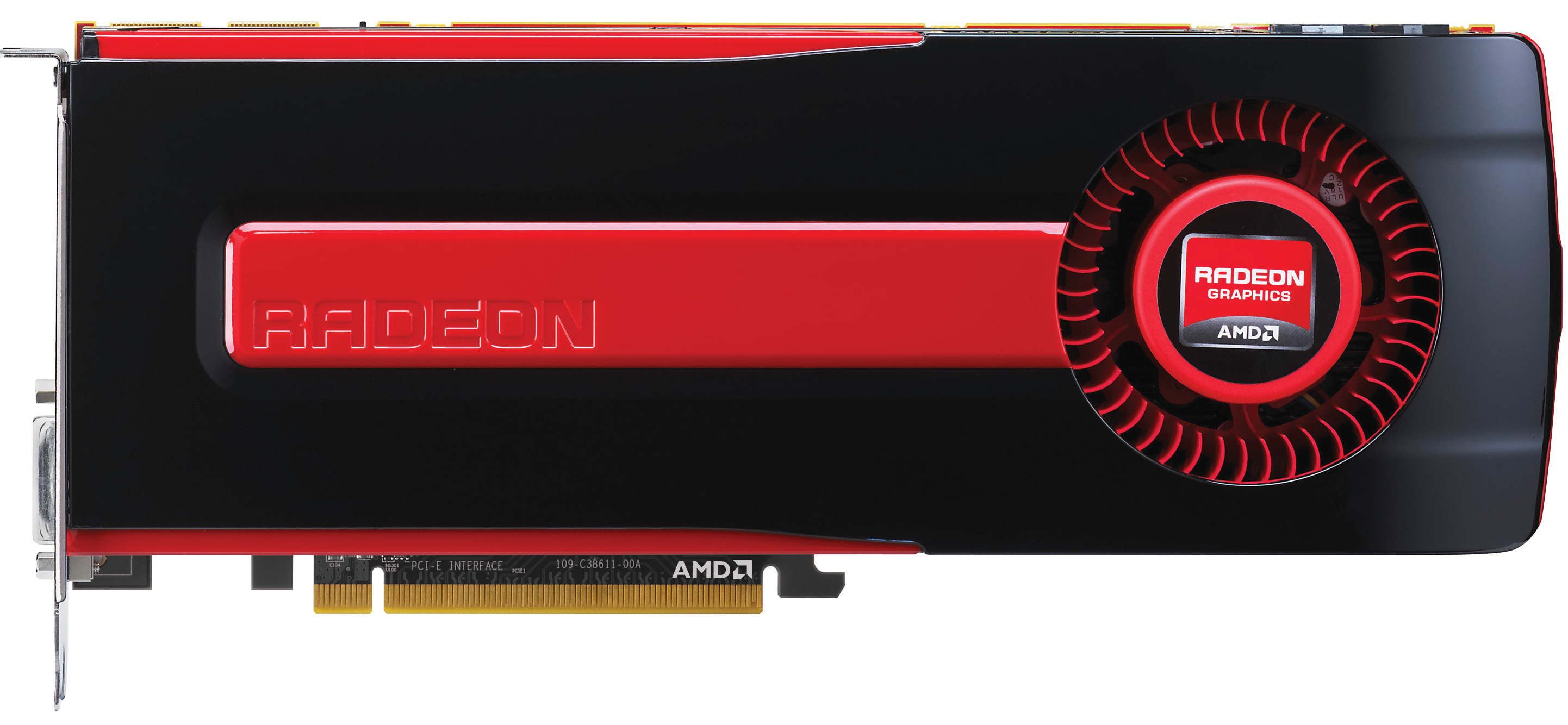
These functional units are joined by a number of other elements, including 8 ROP partitions that can process 32 ROPs per clock, 128 texture units divided up among 32 Compute Units (CUs), and a fixed function pipeline that contains a pair of AMD’s 9th generation geometry engines. Of course all of this hardware would normally take quite a bit of power to run, but thankfully power usage is kept in check by the advancements offered by TSMC’s 28nm process. AMD hasn’t provided us with an official typical board power, but we estimate it’s around 220W, with an absolute 250W PowerTune limit. Meanwhile idle power usage is looking particularly good, as thanks to AMD's further work on power savings their typical power consumption under idle is only 15W. And with AMD's new ZeroCore Power technology (more on that in a bit), idle power usage drops to an asbolutely miniscule 3W.
Overall for those of you looking for a quick summary of performance, the 7970 is quite powerful, but it may not be as powerful as you were expecting. Depending on the game being tested it’s anywhere between 5% and 35% faster than NVIDIA’s GeForce GTX 580, averaging 15% to 25% depending on the specific resolution in use. Furthermore thanks to TSMC’s 28nm process power usage is upwards of 50W lower than the GTX 580, but it’s still higher than the 6970 it replaces. As far as performance jumps go from new fabrication processes, this isn’t as big a leap as we’ve seen in the past.
In a significant departure from the launch of the Radeon HD 5870 and 4870, AMD will not be pricing the 7970 nearly as aggressively as those cards with its launch. The MSRP for the 7970 will be $550, a premium price befitting a premium card, but a price based almost exclusively on the competition (e.g. the GTX 580) rather than one that takes advantage of cheaper manufacturing costs to aggressively undercuts the competition. In time AMD needs to bring down the price of the card, but for the time being they will be charging a price premium reflecting the card’s status as the single-GPU king.
For those of you trying to decide whether to get a 7970, you will have some time to decide. This is a soft launch; AMD will not make the 7970 available until January 9th (the day before the Consumer Electronics Show), nearly 3 weeks from now. We don’t have any idea what the launch quantities will be like, but from what we hear TSMC’s 28nm process has finally reached reasonable yields, so AMD should be in a better position than the 5870 launch. The price premium on the card will also help taper demand side some, though even at $550 this won’t rule out the first batch of cards selling out.
Beyond January 9th, AMD as an entire family of Southern Islands video cards still to launch. AMD will reveal more about those in due time, but as with the Evergreen and Northern Islands families AMD has a plan to introduce a number of video cards over the next year. So 7970 is just the beginning.
| Winter 2011 GPU Pricing Comparison | |||||
| AMD | Price | NVIDIA | |||
| $750 | GeForce GTX 590 | ||||
| Radeon HD 6990 | $700 | ||||
| Radeon HD 7970 | $549 | ||||
| $500 | GeForce GTX 580 | ||||
| Radeon HD 6970 | $350 | GeForce GTX 570 | |||
| Radeon HD 6950 2GB | $250 | ||||
| $240 | GeForce GTX 560 Ti | ||||
| Radeon HD 6870 | $160 | ||||


292 Comments
View All Comments
Scali - Saturday, December 24, 2011 - link
I have never heard Jen-Hsun call the mock-up a working board.They DID however have working boards on which they demonstrated the tech-demos.
Stop trying to make something out of nothing.
Scali - Saturday, December 24, 2011 - link
Actually, since Crysis 2 does not 'tessellate the crap' out of things (unless your definition of that is: "Doesn't run on underperforming tessellation hardware"), the 7970 is actually the fastest card in Crysis 2.Did you even bother to read some other reviews? Many of them tested Crysis 2, you know. Tomshardware for example.
If you try to make smart fanboy remarks, at least make sure they're smart first.
Scali - Saturday, December 24, 2011 - link
But I know... being a fanboy must be really hard these days..One moment you have to spread nonsense about how Crysis 2's tessellation is totally over-the-top...
The next moment, AMD comes out with a card that has enough of a boost in performance that it comes out on top in Crysis 2 again... So you have to get all up to date with the latest nonsense again.
Now you know what the AMD PR department feels like... they went from "Tessellation good" to "Tessellation bad" as well, and have to move back again now...
That is, they would, if they weren't all fired by the new management.
formulav8 - Tuesday, February 21, 2012 - link
Your worse than anything he said. Grow upCeriseCogburn - Sunday, March 11, 2012 - link
He's exactly correct. I quite understand for amd fanboys that's forbidden, one must tow the stupid crybaby line and never deviate to the truth.crazzyeddie - Sunday, December 25, 2011 - link
Page 4:" Traditionally the ROPs, L2 cache, and memory controllers have all been tightly integrated as ROP operations are extremely bandwidth intensive, making this a very design for AMD to use. "
Scali - Monday, December 26, 2011 - link
Ofcourse it isn't. More polygons is better. Pixar subdivides everything on screen to sub-pixel level.That's where games are headed as well, that's progress.
Only fanboys like you cry about it.... even after AMD starts winning the benchmarks (which would prove that Crysis is not doing THAT much tessellation, both nVidia and new AMD hardware can deal with it adequately).
Wierdo - Monday, January 2, 2012 - link
http://techreport.com/articles.x/21404"Crytek's decision to deploy gratuitous amounts of tessellation in places where it doesn't make sense is frustrating, because they're essentially wasting GPU power—and they're doing so in a high-profile game that we'd hoped would be a killer showcase for the benefits of DirectX 11
...
But the strange inefficiencies create problems. Why are largely flat surfaces, such as that Jersey barrier, subdivided into so many thousands of polygons, with no apparent visual benefit? Why does tessellated water roil constantly beneath the dry streets of the city, invisible to all?
...
One potential answer is developer laziness or lack of time
...
so they can understand why Crysis 2 may not be the most reliable indicator of comparative GPU performance"
I'll take the word of professional reviewers.
CeriseCogburn - Sunday, March 11, 2012 - link
Give them a month or two to adjust their amd epic fail whining blame shift.When it occurs to them that amd is actually delivering some dx11 performance for the 1st time, they'll shift to something else they whine about and blame on nvidia.
The big green MAN is always keeping them down.
Scali - Monday, December 26, 2011 - link
Wrong, they showed plenty of demos at the introduction. Else the introduction would just be Jen-Hsun holding up the mock card, and nothing else... which was clearly not the case.They demo'ed Endless City, among other things. Which could not have run on anything other than real Fermi chips.
And yea, I'm really going to go to SemiAccurate to get reliable information!