The AMD Radeon R9 290X Review
by Ryan Smith on October 24, 2013 12:01 AM EST- Posted in
- GPUs
- AMD
- Radeon
- Hawaii
- Radeon 200
Hawaii: Tahiti Refined
Thus far when we’ve been discussing Hawaii, it’s typically been in comparison to Tahiti, and there’s good reason for that. Besides the obvious parallel of being AMD’s new flagship GPU, finally succeeding Tahiti after just short of 2 years, in terms of design Hawaii looks and acts a lot like an improved Tahiti. The underlying architecture is still Graphics Core Next, and a lot of the compute functionality that gave Tahiti its broad applicability to graphics and compute alike is equally present in Hawaii, so in many ways Hawaii looks and behaves like a bigger Tahiti. But as we’ve seen over the years with these second wind parts, there’s are a lot of finer details involved taking an existing architecture and building it bigger, never mind the subtle feature additions that come with Hawaii.
The biggest addition with Hawaii is of course the increased number of functional units. 2 years in and against GPUs like NVIDIA’s GK110, AMD has a clear need to produce a larger, more powerful GPU if they wish to stay competitive with NVIDIA at the high end while also delivering newer, faster products for their regular customers. In doing so there’s a need to identify bottlenecks in the existing design (Tahiti) to figure out what changes will pay off the most for their die size and power consumption cost, and conversely what changes would have little payoff. The end result is that we’re seeing AMD significantly scale up some of the smaller areas of the chip, while taking a more nuanced approach on scaling up the larger areas.
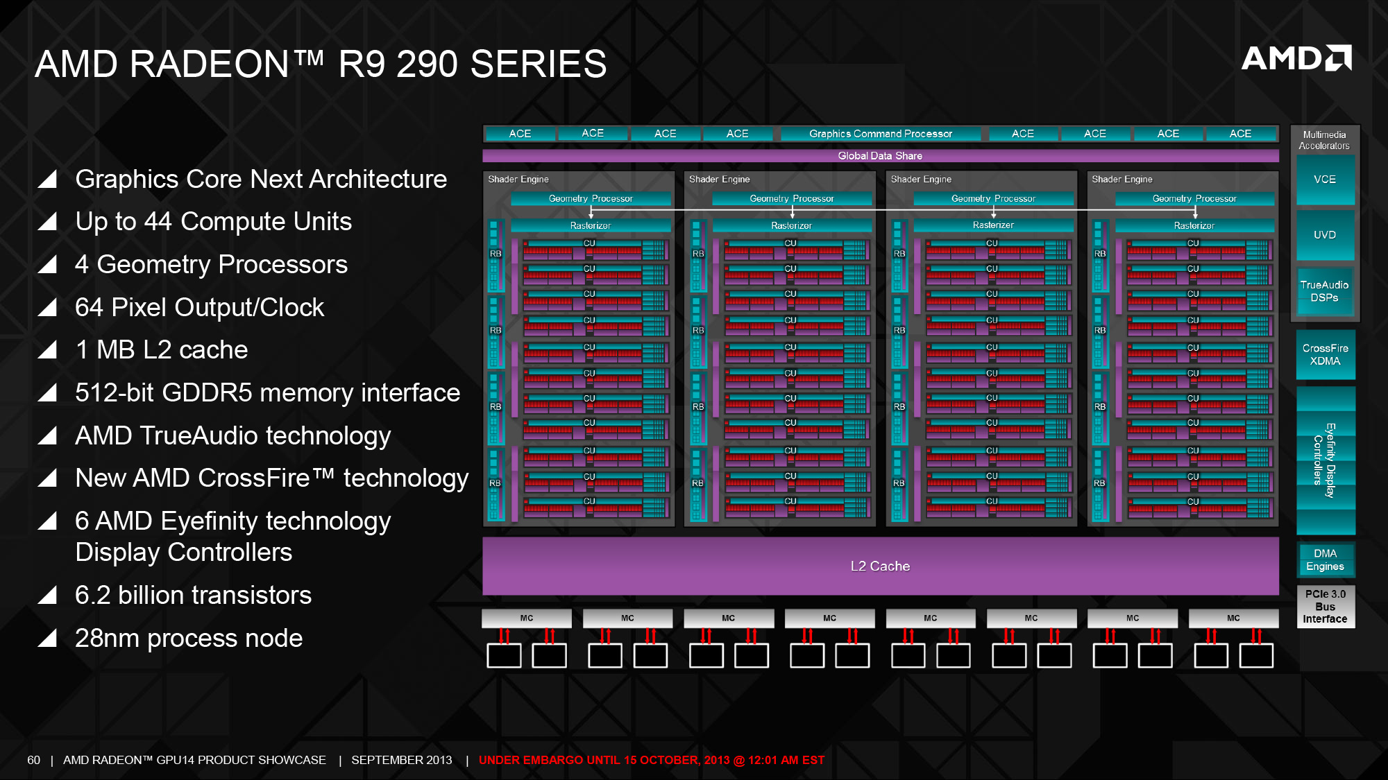
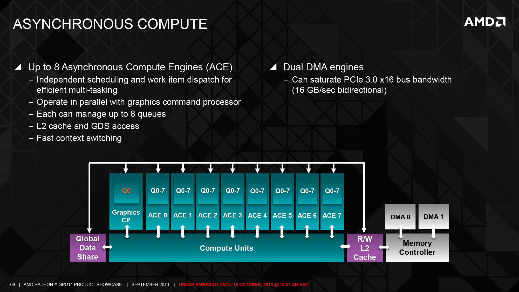
But before we get too deep here, we want to quickly point out that with Hawaii AMD is making a significant change to how they’re logically representing the architecture in public, which although is striking does not mean the underlying low-level organization is nearly as different as the high-level changes would imply. At a high level the biggest change here is that AMD is now segmenting their hardware into “shader engines”. Conceptually the idea is similar to NVIDIA’s SMXes, with each Shader Engine (SE) representing a collection of hardware including shaders/CUs, geometry processors, rasterizers, and L1 cache. Furthermore ROPs are also being worked into the Shader Engine model, with each SE taking on a fraction of the ROPs for the purposes of high level overviews. What remains outside of the SEs is the command processor and ACEs, the L2 cache and memory controllers, and then the various dedicated, non-duplicated functionality such as video decoders, display controllers, DMA controllers, and the PCIe interface.
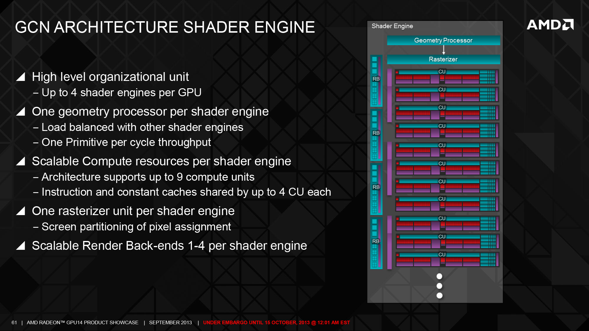
Moving forward, AMD designs are going to scale up and down both with respect to the number of SEs and in the number of CUs in each SE. This distinction is important because unlike NVIDIA’s SMX model, where the company can only scale down hardware by cutting whole SMXes, AMD can technically maintain up to 4 SEs while scaling down the number of CUs within each SE. So despite what the SE model implies, AMD’s scaling abilities are status quo for GCN in as much as they can continue to scale down for lower tier parts without sacrificing geometry or ROP performance. In reality of course the physical layout of Hawaii and other GPUs will deviate by even less, as the ROPs are still going to be tied into the memory controllers, the geometry processors are still closely integrated with the command processor, etc. Still, as a high level model it’s likely a better fit for how the underlying hardware really works, as it provides a more intuitive view on how the number of geometry processors, rasterizers, and ROPs are closedly related, or how the individual CUs are lumped together into CU arrays.
With that in mind, we’ll start or low level overview with a look at both the front end and the back end of Hawaii. Of all the aspects of the GPU AMD has scaled up compared to Hawaii, it’s at the front end and the back end that we’ll find the biggest changes due to the fact that AMD has doubled the number of functional units in most of the elements that reside here.
At the very front, in conjunction with the ACE improvements inherient to GCN 1.1, AMD has scaled up the number of ACEs from 2 in Tahiti to 8 in Hawaii. With each ACE now containing 8 work queues this brings the total number of work queues to 64. Unlike most of the other changes we’ll be going over today, the ACE increase has limited applicability for gaming, and while AMD isn’t talking about non-Radeon Hawaii products at this time, given what we know about GCN 1.1 there’s a clear applicability not only towards HSA, but also to more traditional GPU compute setups such as the FirePro S series. For GPU compute the additional ACEs and queues will help improve AMD’s real world compute performance by improving the utilization of the CUs, while the DMA engine improvements that come with the increased number of ACEs will help keep the CUs fed with data from the CPU and other GPUs.
Moving on, there are a number of back end and front end changes AMD has made to improve rendering performance, and the increased number of geometry processors is at the forefront of this. With Hawaii AMD has doubled the number of geometry engines from 2 to 4, and more closely coupling those with the existing 4 rasterizer setup they inherit. The increase in geometry processors comes at an appropriate time for the company as the last time the number of geometry processors was increased was with the 6900 series in 2010, when the company moved to 2 such processors. One of the side effects of the new consoles coming out this year is that cross-platform games will be able to use a much larger number of primitives than before – especially with the uniform addition of D3D11-style tessellation – so there’s a clear need to ramp up geometry performance to keep up with where games are expected to go.

Further coupled with this are more generalized improvements designed to improve geometry efficiency overall. Alongside the additional geometry processors AMD has also improved both on-chip and off-chip data flows, with off-chip buffering being improved to further improve AMD’s tessellation performance, while the Local Data Store can now be tapped by geometry shaders to reduce the need to go off-chip at all. More directly applicable is that the inter-stage storage (parameter and position caches) used by the geometry processors has also been increased in order to keep up with the overall increase in the number of processors.
On a side note, with every architectural revision/launch we try to get AMD’s engineers to give us an idea of what aspects they’re most proud of, and while they typically downplay the question (it’s a team effort, after all) for Hawaii the geometry processor changes have been a recurring theme of something where the engineering team is particularly proud of its work. As it turns out adding geometry processors is actually a quite a bit harder than it sounds, as the additional processors bring with it the need to balance geometry workloads across the processor cluster. When splitting up the geometry workload there are dependency issues that must be addressed, and to maximize efficiency there are load balancing/partitioning matters that must be taken into account as there’s no guarantee geometry is evenly distributed over the entire viewport. Consequently AMD’s engineers are quite happy with how this turned out due to the effort involved.
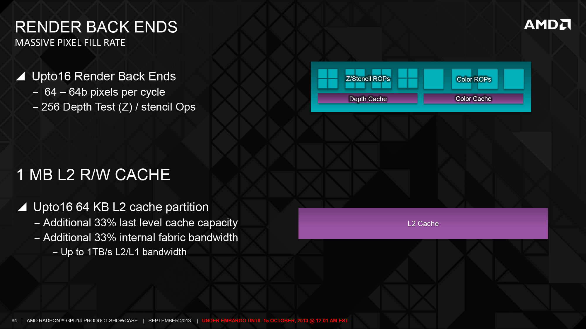
Meanwhile at the other end of the rendering pipeline we have AMD’s back end changes, which have been made in concert with the changes to the front end. The big change here is that for the first time since the 5870 (Cypress) back in 2009, AMD has increased the number of ROPs, going from 32 on Tahiti/Pitcairn to 64 on Hawaii. As ROPs are primarily tasked with jobs that are resolution dependent such as final pixel resolution and depth testing, the workload placed on ROPs has increased much more slowly over the years than the workload placed on shaders or even geometry processors. Similarly, for that reason scaling up the ROPs alone typically doesn’t have a big impact on rendering performance, hence ROP upgrades have come far more sparingly.
With Hawaii the increase in the number of ROPs comes down to a few different factors. To a large extent it’s merely a matter of “it’s time”, where the performance increases finally justify the die space increases. But AMD’s focus on 4K resolution workloads also plays a significant part, as 4K represents a significant increase in the ROP workload, and hence the need for more ROPs to pick up the work. Consequently while we can’t easily compare ROP performance across vendors, increasing the number of ROPs is one of the ways AMD will extend their high resolution performance advantage over NVIDIA, by being sure they have plenty of capacity to chew through 4K scenes.
Working in conjunction with the ROPs of course is the L2 cache, forming the second member of the ROP/L2/MC triumvirate, and like the number of ROPs this is being increased. L2 cache is more closely tied to the memory controllers than the ROPs, so while Tahiti had 32 ROPs and 768KB of L2 paired with 6 memory controllers, Hawaii gets double the ROPs but a smaller 33% increase in the L2 cache in accordance with the 33% increase in memory controllers. The end result is that Hawaii packs a full 1MB of L2 cache, and that the total bandwidth available out of the L2 cache has also been increased by 33% to a full 1TB. The L2 cache plays a role in every aspect of rendering, and as the primary backstop for the ROPs and secondary backstop for the CUs it’s critical to avoiding relatively expensive off-chip memory operations.
Lastly we have the final member of the ROP/L2/MC triumvirate, which is the memory interface. Tahiti for all of its strengths and weaknesses possesses a very large memory interface (as a percentage of die space), which has helped it reach 6GHz+ memory speeds on a 384-bit memory bus at the cost of die size. As there’s a generally proportional relationship between memory interface size and memory speeds, AMD has made the interesting move of going the opposite direction for Tahiti. Rather than scale up a 384-bit memory controller even more, they opted to scale down an even larger 512-bit memory controller with impressive results.
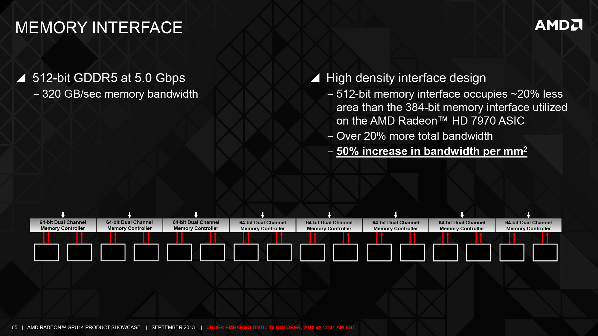
The result of AMD’s memory interface changes is that between the die space savings from the lower speed controllers coupled with a number of smaller tweaks to improve density, AMD has been able to implement the larger 512-bit memory interface while still reducing the size of the memory interface by 20% as compared to Tahiti. Furthermore these space savings still allow for a meaningful increase in memory bandwidth despite the lower memory clockspeeds, with AMD being able to increase their memory bandwidth by over 10% (as compared to 280X), from 288GB/sec to 320GB/sec. The end result is a very neat and clean (and impressive) improvement in AMD’s memory controllers, with AMD reducing their interface size and increasing their memory bandwidth at the same time. The 512-bit memory bus does have some externalities to it – specifically increased PCB costs and requiring more GDDR5 memory modules than Tahiti (16 vs. 12) – but these are ultimately countered by the die space savings that AMD is realizing from the smaller memory interface.
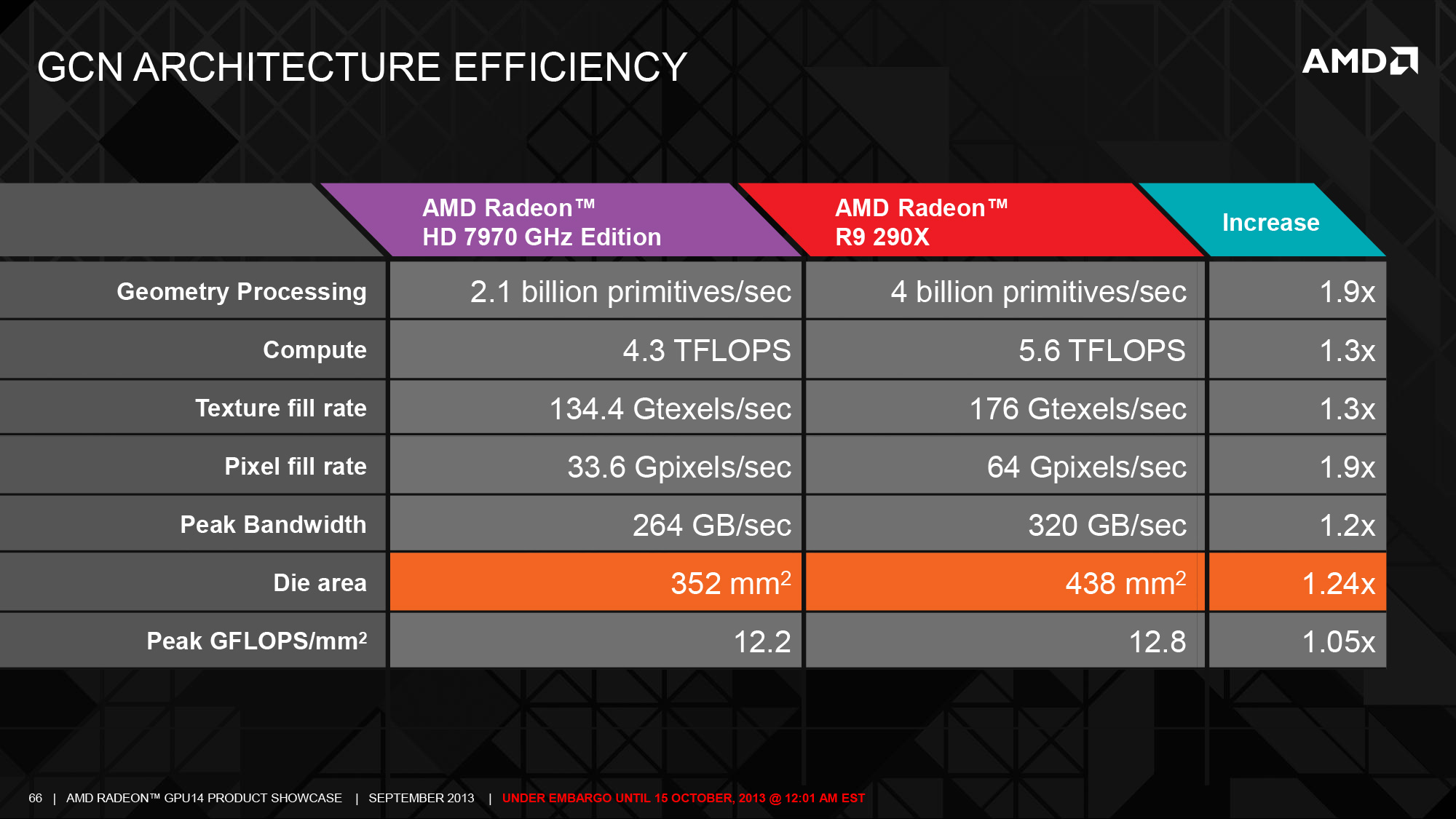
Meanwhile compared to AMD’s front end and back end changes, the Hawaii’s CU changes are much more straightforward. Besides optimizing the CUs for die size and giving them the appropriate GCN 1.1 functionality, very little has changed here. The end result is a simple increase in the number of CUs, going from 32 on Tahiti to 44 on Hawaii, with AMD continuing to distribute them evenly over the 4 Shader Engines. Shading/texturing remains the primary bottleneck for most games today, so while the CU increase is straightforward the performance implications are not to be ignored. Much of AMD’s 30% performance increase comes from this 38% increase in CUs. GCN was after all designed from the start to scale up well in this respect, so with Hawaii AMD is executing on those plans.
Moving on, having completed our look at the design of Hawaii, let’s discuss the die size of Hawaii a bit. Unlike NVIDIA, AMD doesn’t traditionally go above 400mm2 dies, and for good reason. NVIDIA holds the lion’s share of the high end, high margin workstation market, and while AMD market share has been slowly increasing from the historic lows of a couple of years ago it’s still well behind NVIDIA’s. Consequently AMD doesn’t have that high margin market to help bootstrap the production of large GPUs, requiring that they stay smaller to stay within their means.
With Hawaii AMD still isn’t entering the big die race that defines NVIDIA’s flagship GPUs, but AMD is going larger than ever before. At 438mm2 Hawaii is AMD’s biggest GPU yet, and despite AMD’s improvements in area efficiency Hawaii is still 73mm2 (20%) larger than Tahiti. The fact that AMD is able to improve their gaming performance by 30% over Tahiti means that this is a very good tradeoff to make, it just means that AMD is treading new ground in doing so.
Similarly, at 6.2 billion transistors Hawaii is AMD’s largest GPU yet by transistor count, outpacing the 4.31B Tahiti by 1.89B transistors, an increase of 44%. Now transistor counts alone don’t mean much, but the fact that AMD was able to increase their transistor density by this much is a significant accomplishment for the company.
Meanwhile on a historical basis it’s worth pointing out that while AMD’s “small die” strategy effectively died with Cayman in 2010, this marks the first time since R600 that AMD has dared to go this big. R600, AMD’s previously largest GPU, ended up being rather ill-fated, which in turn spurred on the small die strategy that defined the R700 and Evergreen GPU families. Hawaii won’t be a repeat of R600 – in particular AMD isn’t going to be repeating the unfortunate circumstance of building a large GPU against a new architecture and a new manufacturing node all at the same time – so they are certainly on far more solid ground this time. Ultimately the success of Hawaii will be based on sales and profit margins as always, but based on the performance we’re seeing and the state of AMD’s market, AMD shouldn’t have any trouble justifying a 400mm2 GPU at this point. This is yet another benefit of being a second wind product: AMD gets to build their large GPU against a mature manufacturing process, as opposed to the immature process that Tahiti had to work with.


396 Comments
View All Comments
Sandcat - Thursday, October 24, 2013 - link
Perhaps they knew it was unsustainable from the beginning, but short term gains are generally what motivate managers when the develop pricing strategies, because bonus. Make hay whilst the sun shines, or when AMD is 8 months late.chizow - Saturday, October 26, 2013 - link
Possibly, but now they have to deal with the damaged goodwill of some of their most enthusiastic, spendy customers. I can't count how many times I've seen it, someone saying they swore off company X or company Y because they felt they got burned/screwed/fleeced by a single transaction. That is what Nvidia will be dealing with going forward with Titan early adopters.Sancus - Thursday, October 24, 2013 - link
AMD really needs to do better than a response 8 months later to crash anyone's parade. And honestly, I would love to see them put up a fight with Maxwell at a reasonable time period so they have incentive to keep prices lower. Otherwise, expect Nvidia to "overprice" things next generation as well.When they have no competition for 8 months it's not unsustainable to price as high as the market will bear, and there's no real evidence that Titan was economically overpriced because it's not like there was a supply glut of Titans sitting around anywhere, in fact they were often out of stock. So really, Nvidia is just pricing according to the market -- no competition from AMD for 8 months, fastest card with limited supply, why WOULD they price it at anything below $1000?
chizow - Saturday, October 26, 2013 - link
My reply would be that they've never had to price it at $1000 before, and we have certainly seen this level of advancement from one generation to the next in the past (7900GTX to 8800GTX, 8800GTX to GTX 280, 280 GTX to 480 GTX, etc), so it's not completely ground-breaking performance increases even though Kepler overall outperformed historical improvements by ~20%, imo.Also, the concern with Titan isn't just the fact it was priced at ungodly premiums this time around, it's the fact it held it's crown for such a relatively short period of time. Sure Nvidia had no competition at the $500+ range for 8 months, but that was also the brevity of Titan's reign at the top. In the past, a flagship in that $500 or $600+ range would generally reign for the entire generation, especially one that was launched half way through that generation's life cycle. Now Nvidia has already announced a reply with the 780 Ti which will mean not one, but TWO cards will surpass Titan at a fraction of it's price before the generation goes EOL.
Nvidia was clearly blind-sided by Hawaii and ultimately it will cost them customer loyalty, imo.
ZeDestructor - Thursday, October 24, 2013 - link
$1000 cards are fine, since the Titan is a cheap compute unit compared to the Quadro K6000 and the 690 is a dual-GPU card (Dual-GPU has always been in the $800+ range).What we should see is the 780 (Ti?) go down in price and match the R9-290x, much to the rejoicing of all!
Nvidia got away with $650-750 on the 780 because they could, and THAT is why competition is important, and why I pay attention to AMD even if I have no reason to buy from them over Nvidia (driver support on Linux is a joke). Now they have to match. Much of the same happens in the CPU segement.
chizow - Saturday, October 26, 2013 - link
For those that actually bought the Titan as a cheap compute card, sure Titan may have been a good buy, but I doubt most Titan buyers were buying it for compute. It was marketed as a gaming card with supercomputer guts and at the time, there was still much uncertainty whether or not Nvidia would release a GTX gaming card based on GK110.I think Nvidia preyed on these fears and took the opportunity to launch a $1K part, but I knew it was an unsustainable business model for them because it was predicated on the fact Nvidia would be an entire ASIC ahead of AMD and able to match AMD's fastest ASIC (Tahiti) with their 2nd fastest (GK104). Clearly Hawaii has turned that idea on it's head and Nvidia's premium product stack is crashing down in flames.
Now, we will see at least 4 cards (290/290X, 780/780Ti) that all come close to or exceed Titan performance at a fraction of the price, only 8 months after it's launch. Short reign indeed.
TheJian - Friday, October 25, 2013 - link
The market dictates pricing. As they said, they sell every Titan immediately, so they could probably charge more. But that's because it has more value than you seem to understand. It is a PRO CARD at it's core. Are you unaware of what a TESLA is for $2500? It's the same freaking card with 1 more SMX and driver support. $1000 is GENEROUS whether you like it or not. Gamers with PRO intentions laughed when they saw the $1000 price and have been buying them like mad ever since. No parade has been crashed. They will continue to do this pricing model for the foreseeable future as they have proven there is a market for high-end gamers with a PRO APP desire on top. The first run was 100,000 and sold in days. By contrast Asus Rog Ares 2 had 1000 unit first run and didn't sell out like that. At $1500 it really was a ripoff with no PRO side.I think they'll merely need another SMX turned on and 50-100mhz for the next $1000 version which likely comes before xmas :) The PRO perf is what is valued here over a regular card. Your short-lived statement makes no sense. It's been 8 months, a rather long life in gpus when you haven't beaten the 8 month old card in much (I debunked 4k crap already, and pointed to a dozen other games where titan wins at every res). You won't fire up Blender, Premiere, PS CS etc and smoke a titan with 290x either...LOL. You'll find out what the other $450 is for at that point.
chizow - Saturday, October 26, 2013 - link
Yes and as soon as they released the 780, the market corrected itself and Titans were no longer sold out anywhere, clearly a shift indicating the price of the 780 was really what the market was willing to bear.Also, there are more differences with their Tesla counterparts than just 1 SMX, Titan lacks ECC support which makes it an unlikely candidate for serious compute projects. Titan is good for hobby compute, anything serious business or research related is going to spend the extra for Tesla and ECC.
And no, 8-months is not a long time at the top, look at the reigns of previous high-end parts and you will see it is generally longer than this. Even the 580 that preceded it held sway for 14-months before Tahiti took over it's spot. Time at the top is just one part though, the amount which Titan devalued is the bigger concern. When 780 launched 3 months after Titan, you could maybe sell Titan for $800. Now that Hawaii has launched, you could maybe sell it for $700? It's only going to keep going down, what do you think it will sell for once 780Ti beats it outright for $650 or less?
Sandcat - Thursday, October 24, 2013 - link
I noticed your comments on the Tahiti pricing fiasco 2 years ago and generally skip through the comment section to find yours because they're top notch. Exactly what I was thinking with the $550 price point, finally a top-tier card at the right price for 28nm. Long live sanity.chizow - Saturday, October 26, 2013 - link
Thanks! Glad you appreciated the comments, I figured this business model and pricing for Nvidia would be unsustainable, but I thought it wouldn't fall apart until we saw 20nm Maxwell/Pirate Islands parts in 2014. Hawaii definitely accelerated the downfall of Titan and Nvidia's $1K eagle's nest.