The NVIDIA GeForce GTX 750 Ti and GTX 750 Review: Maxwell Makes Its Move
by Ryan Smith & Ganesh T S on February 18, 2014 9:00 AM EST
As the GPU company who’s arguably more transparent about their long-term product plans, NVIDIA still manages to surprise us time and time again. Case in point, we have known since 2012 that NVIDIA’s follow-up architecture to Kepler would be Maxwell, but it’s only more recently that we’ve begun to understand the complete significance of Maxwell to the company’s plans. Each and every generation of GPUs brings with it an important mix of improvements, new features, and enhanced performance; but fundamental shifts are fewer and far between. So when we found out Maxwell would be one of those fundamental shifts, it changed our perspective and expectations significantly.
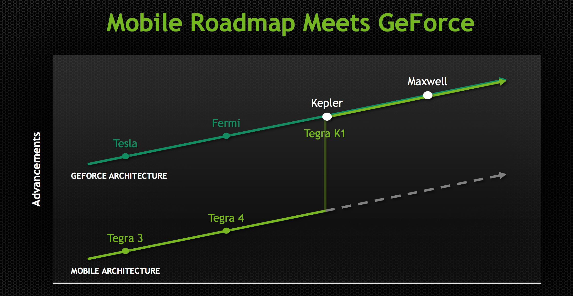
What is that fundamental shift? As we found out back at NVIDIA’s CES 2014 press conference, Maxwell is the first NVIDIA GPU that started out as a “mobile first” design, marking a significant change in NVIDIA’s product design philosophy. The days of designing a flagship GPU and scaling down already came to an end with Kepler, when NVIDIA designed GK104 before GK110. But NVIDIA still designed a desktop GPU first, with mobile and SoC-class designs following. However beginning with Maxwell that entire philosophy has come to an end, and as NVIDIA has chosen to embrace power efficiency and mobile-friendly designs as the foundation of their GPU architectures, this has led to them going mobile first on Maxwell. With Maxwell NVIDIA has made the complete transition from top to bottom, and are now designing GPUs bottom-up instead of top-down.
Nevertheless, a mobile first design is not the same as a mobile first build strategy. NVIDIA has yet to ship a Kepler based SoC, let alone putting a Maxwell based SoC on their roadmaps. At least for the foreseeable future discrete GPUs are going to remain as the first products on any new architecture. So while the underlying architecture may be more mobile-friendly than what we’ve seen in the past, what hasn’t changed is that NVIDIA is still getting the ball rolling for a new architecture with relatively big and powerful GPUs.
This brings us to the present, and the world of desktop video cards. Just less than 2 years since the launch of the first Kepler part, the GK104 based GeForce GTX 680, NVIDIA is back and ready to launch their next generation of GPUs as based on the Maxwell architecture.
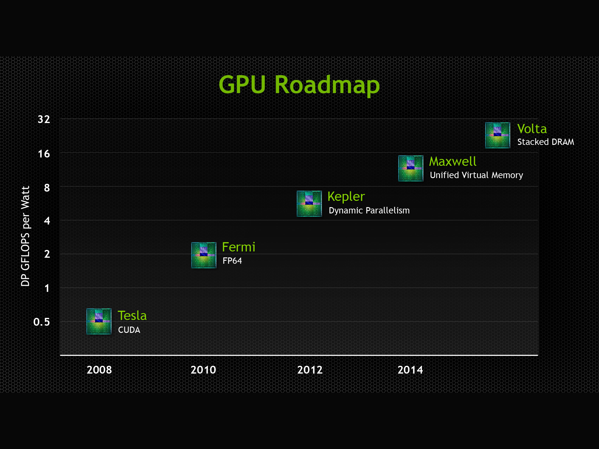
No two GPU launches are alike – Maxwell’s launch won’t be any more like Kepler’s than Kepler was Fermi’s – but the launch of Maxwell is going to be an even greater shift than usual. Maxwell’s mobile-first design aside, Maxwell also comes at a time of stagnation on the manufacturing side of the equation. Traditionally we’d see a new manufacturing node ready from TSMC to align with the new architecture, but just as with the situation faced by AMD in the launch of their GCN 1.1 based Hawaii GPUs, NVIDIA will be making do on the 28nm node for Maxwell’s launch. The lack of a new node means that NVIDIA would either have to wait until the next node is ready, or launch on the existing node, and in the case of Maxwell NVIDIA has opted for the latter.
As a consequence of staying on 28nm the optimal strategy for releasing GPUs has changed for NVIDIA. From a performance perspective the biggest improvements still come from the node shrink and the resulting increase in transistor density and reduced power consumption. But there is still room for maneuvering within the 28nm node and to improve power and density within a design without changing the node itself. Maxwell in turn is just such a design, further optimizing the efficiency of NVIDIA’s designs within the confines of the 28nm node.
With the Maxwell architecture in hand and its 28nm optimizations in place, the final piece of the puzzle is deciding where to launch first. Thanks to the embarrassingly parallel nature of graphics and 3D rendering, at every tier of GPU – from SoC to Tesla – GPUs are fundamentally power limited. Their performance is constrained by the amount of power needed to achieve a given level of performance, whether it’s limiting clockspeed ramp-ups or just building out a wider GPU with more transistors to flip. But this is especially true in the world of SoCs and mobile discrete GPUs, where battery capacity and space limitations put a very hard cap on power consumption.
As a result, not unlike the mobile first strategy NVIDIA used in designing the architecture, when it comes to building their first Maxwell GPU NVIDIA is starting from the bottom. The bulk of NVIDIA’s GPU shipments have been smaller, cheaper, and less power hungry chips like GK107, which for the last two years has formed the backbone of NVIDIA’s mobile offerings, NVIDIA’s cloud server offerings, and of course NVIDIA’s mainstream desktop offerings. So when it came time to roll out Maxwell and its highly optimized 28nm design, there was no better and more effective place for NVIDIA to start than with the successor to GK107: the Maxwell based GM107.
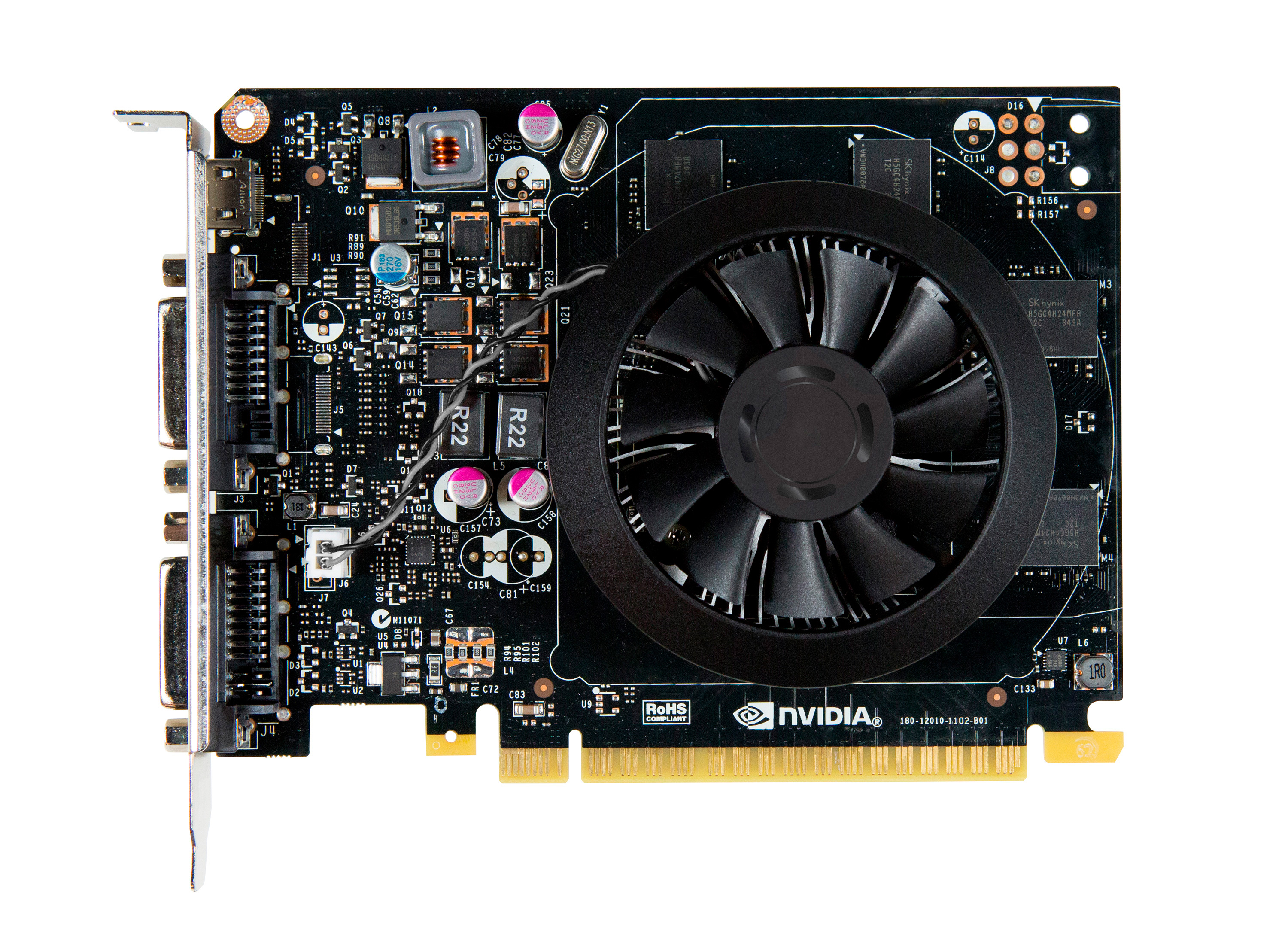
Over the coming months we’ll see GM107 in a number of different products. Its destiny in the mobile space is all but set in stone as the successor to the highly successful GK107, and NVIDIA’s GRID products practically beg for greater efficiency. But for today we’ll be starting on the desktop with the launch of NVIDIA’s latest desktop video cards: GeForce GTX 750 Ti and GeForce GTX 750.


177 Comments
View All Comments
Mondozai - Wednesday, February 19, 2014 - link
Anywhere outside of NA gives normal prices. Get out of your bubble.ddriver - Wednesday, February 19, 2014 - link
Yes, prices here are pretty much normal, no on rushes to waste electricity on something as stupid as bitcoin mining. Anyway, I got most of the cards even before that craze began.R3MF - Tuesday, February 18, 2014 - link
at ~1Bn transitors for 512Maxwell shaders i think a 20nm enthusiast card could afford the 10bn transistors necessary for a 4096 shaders...Krysto - Tuesday, February 18, 2014 - link
If Maxwell has 2x the P/W, and Tegra K2 arrives at 16nm, with 2 SMX (which is very reasonable expection), then Tegra K2 will have at least a 1 Teraflop of performance, if not more than 1.2 Teraflops, which would already surpass the Xbox One.Now THAT's exciting.
chizow - Tuesday, February 18, 2014 - link
It probably won't be Tegra K2, will most likely be Tegra M1 and could very well have 3xSMM at 20nm (192x2 vs. 128x3), which according to the article might be a 2.7x speed-up vs. just a 2x using Kepler's SMX arch. But yes, certainly all very exciting possibilities.grahaman27 - Wednesday, February 19, 2014 - link
the Tegra M1 will be on 16nm finfet if they stick to their roadmap. But, since they are bringing the 64bit version sooner than expected, I dont know what to expect. BTW, it has yet to be announce what manufacturing process the 64bit version will be... we can only hope TSMC 20nm will arrive in time.Mondozai - Wednesday, February 19, 2014 - link
Exciting or f%#king embarrassing for M$? Or for the console industry overall.RealiBrad - Tuesday, February 18, 2014 - link
Looks to be an OK card when you consider that mining has caused AMD cards to sell out and push up price.It looks like the R7 265 is fairly close on power, temp, and noise. If AMD supply could meet demand, then the 750Ti would need to be much cheaper and would not look nearly as good.
Homeles - Tuesday, February 18, 2014 - link
Load power consumption is clearly in Nvidia's favor.DryAir - Tuesday, February 18, 2014 - link
Power consumpion is way higher... give a look at TPU´s review. But price/perf is a lot beter yeah.Personally I'm a sucker for low power, and I will gadly pay for it.