Testing Samsung 850 Pro Endurance & Measuring V-NAND Die Size
by Kristian Vättö on July 7, 2014 1:20 PM EST
Last week Samsung announced the 850 Pro, which is the first mainstream SSD to utilize 3D V-NAND. We already reviewed the drive and covered the fundamentals of V-NAND in detail but there is one thing I did not have the time to test: endurance. The most promising aspect of V-NAND is its increased endurance and Samsung has claimed endurance of up to ten times of 2D NAND. However, the 850 Pro is only rated at 150TB, which is twice the rating of 840 Pro, so I wanted to dig deeper and determine the endurance rating in terms of program/erase cycles.
To calculate the P/E cycles, I used a method similar to what we used with the SSD 840 two years ago. Basically, I wrote 128KB sequential data (QD1) to the drive and wrote down the necessary SMART values as well as the average throughput after every test. After repeating the test over a dozen times, I had enough data to figure out the P/E cycle count.
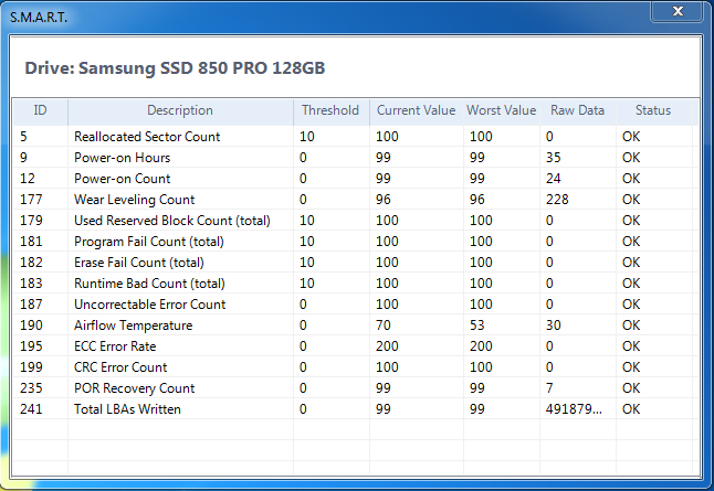
The Wear Leveling Count (WLC) SMART value gives us all the data we need. The current value stands for the remaining endurance of the drive in percentage, meaning that it starts from 100 and decreases linearly as the drive is written to. The raw WLC value counts the consumed P/E cycles, so if these two values are monitored while writing to the drive, sooner than later we will find the spot where the normalized value drops by one.
I found that the current WLC value drops by one after 60 P/E cycles (I ran the test over multiple WLC drops), which suggests that the WLC will drop to zero after 6,000 P/E cycles. In other words, the V-NAND in 850 Pro is good for 6,000 P/E cycles, which is twice the cycle count of modern 2D MLC NAND but quite far away from Samsung's "ten times the endurance" claims. Either Samsung is using lower binned parts in the 850 Pro (i.e. saving the 30,000 P/E cycle parts for enterprise drives) or the WLC value has artificially been limited to ensure that enterprises do not use the 850 Pro and pay the premium for the 845DC EVO/Pro instead. I am thinking it is more of the latter because the enterprise drives bring home much higher profits and of course Samsung wants to make sure that the 850 Pro is not used outside the client environment.
Once WLC reaches zero or one, it is generally a good idea to replace the drive as it may no longer be reliable. However, that does not mean that the drive will immediately fail -- according to JEDEC spec the P/E cycle rating is with one-year data retention, meaning that there can still be plenty of life left. The Tech Report's endurance testing gives a good picture of how much you can write after the WLC drops to zero, although personally I would still replace the drive ASAP because there is no guarantee that each drive performs similarly (remember, NAND is binned for endurance so there can be differences).
| SSD Lifetime Estimation | ||||
| 128GB | 256GB | 512GB | 1TB | |
| Raw NAND Capacity | 129GiB | 258GiB | 516GiB | 1032GiB |
| NAND P/E Cycles | 6,000 | |||
| Raw NAND Endurance | 755.9TiB | 1,511.7TiB | 3,023.4TiB | 6,046.9TiB |
| Lifespan with 20GiB of Host Writes per Day with 1.5x Write Amplification | 35.34 years | 70.68 years | 141.37 years | 282.74 years |
| Lifespan with 100GiB of Host Writes per Day with 3x Write Amplification | 7.07 years | 14.14 years | 28.27 years | 56.55 years |
| Drive Writes per Day with 5x Write Amplification | 1.10 | 1.10 | 1.10 | 1.10 |
The above table gives a good summary of how durable the 850 Pro really is. Even if you write 100GiB (GB in Windows is really GiB, i.e. 1024^3 bytes) per day with a write amplification of three, the smallest 128GB model will last for over seven years. 100GiB per day is very rare in a client environment and to be honest I can only see this applying to some high-end media professionals that use the drive for production purposes. On the other hand, media professionals will likely spring for a larger capacity anyway as 128GB might not even be capable of holding the data of one project. For a more typical user there is absolutely nothing to worry about as the 850 Pro will likely outlive the rest of the components.
Of course, there is still the 150TB write limitation on the warranty. That figure is based on host writes, so it applies even if you are only writing sequential data with low write amplification. Samsung did, however, tell me that they can make exceptions as long as the drive is used in client environment, meaning that the purpose of the endurance rating is mostly to make sure that the 850 Pro is not used in write intensive enterprise applications.
Testing Write Amplification
In addition to testing the endurance, I decided to see what the worst-case write amplification looks like. The test regime is similar to the endurance testing but the writes are 4KB random (QD32) to illustrate the worst possible scenario for the drive. Unfortunately, Samsung's SMART values do not report total NAND writes like Intel does, but the raw Wear Leveling Count basically gives us NAND writes in increments of the capacity of the drive (one P/E cycle = 129GiB of NAND writes for the 128GB drive). I recorded the Wear Leveling Count as well as the Total LBAs Written (i.e. host writes) value while writing 4KB random data to the drive.
| Worst-Case Write Amplification | |
| Host Writes | 493.9GiB |
| P/E Cycles Consumed | 42 |
| Approximate NAND Writes | 5,418GiB |
| Observed Write Amplification | 10.97x |
About 10x worst-case write amplification is fairly typical for a moden client SSD. Fortunately the days of +100x write amplification are over and under common client workloads the write amplification will usually stay below 2x.
| Worst-Case Endurance | ||||
| 128GB | 256GB | 512GB | 1TB | |
| Write Amplification | 11x | |||
| Total Bytes Written (TBW) | 68.7TiB | 137.4TiB | 274.9TiB | 549.7TiB |
| Drive Writes per Day for 5 Years | 0.43 | 0.43 | 0.43 | 0.43 |
The table above is just to show how the 850 Pro would bear in worst-case scenario that may be relevant to some enterprise users. I will be putting the 850 Pro through our enterprise test suite to see how it stacks up in terms of performance but especially with added over-provisioning, I can see the 850 Pro being viable for some read intensive enterprise workloads.


39 Comments
View All Comments
isa - Monday, July 7, 2014 - link
A thoughtful article, Kristian. As an ex-ASIC designer, I agree with your assessment that the SMART value is likely being manipulated by Samsung - no competent IC fab would have the bimodal yield variability that would otherwise account for the 2x SMART value versus the 10x marketing claim. If the result was in fact based on yield variability, then you'd see a range of SMART decimation values for a range of samples. But if all the drives report a consistent 2x effect, then it's being manipulated.emvonline - Monday, July 7, 2014 - link
Great article and comments Kristian! just what I was looking for.... Thanks!The lateral spacing is far larger than expected with 40nm lithography and hence the cell density is much lower than expected for theoretical VNAND.
Most companies think 3D NAND makes sense only with 256Gbit to be cost effective. Lower densities get expensive due to array efficiency. IMO, Samsung is introducing a new part at high cost and high price so they can fix efficiencies later. smart move
FunBunny2 - Monday, July 7, 2014 - link
With regard to the 2X and 10X issue. Is Samsung claiming both numbers, in different places, specifically to NAND performance? Or is "endurance" an SSD number, which would encompass controller logic, spare area, and such, thus 10X while raw NAND performance is 2X?mkozakewich - Tuesday, July 8, 2014 - link
In the world of enterprise and the government, you don't generally want things failing unexpectedly. Most tolerance standards incorporate that truth, so you get ratings that aren't even close to failure at their maximums.I assume that's what's going on here. It seems weird that AnandTech is acting incredulous about it, because they specifically called it out when testing other (Intel, I think?) drives. Basically, the wear-levelling factor usually means nothing. Like an expiry date on milk, you can be statistically assured that nearly all the products will be fine within that boundary. That the number is so low on these SSDs makes me think there's a large amount of variance in their samples, and it has to be that low to catch a high enough percentage to fit their failure tolerance.
That and I *think* they got the 10x number from a single drive Samsung was boasting about.
Sivar - Wednesday, July 9, 2014 - link
Units missing. Please add.1.10 what per day? 0.43 what?
Kristian Vättö - Thursday, July 10, 2014 - link
Drive writes per day, it's mentioned in the left-hand side column.LordConrad - Wednesday, July 9, 2014 - link
"... (GB in Windows is really GiB, i.e. 1024^3 bytes)..."Windows is correct to use GB. When a prefix (Giga) is used in front of a binary measurement (Byte), the resulting measurement remains binary. Hard drive manufacturers use of the prefixes is wrong (and done for the sole purpose of inflating their numbers), Windows is right, and GiB is a redundant measurement.
Zan Lynx - Wednesday, July 16, 2014 - link
You are right in your own imagination.SI units are SI units, period, end, stop.
sonicmerlin - Thursday, July 10, 2014 - link
Does this mean Samsung could deploy V-NAND on a 1X nm process and effect a 32x increase in density? Or even 2X nm process and 16x density increase? That would put them ahead of HDDs in terms of cost per bit, wouldn't it? Is there any reason they're not going down this path in at least the consumer market, where SSD endurance isn't a top priority?garadante - Friday, July 11, 2014 - link
Probably because they have no reason to absolutely crash the price/GB standard for SSDs. They'd have absolutely no competitors at that density in the immediate future so nobody could compete. And considering their current model allows them to just barely eke out densities ahead of competitors in order to give them the most competitive product (if barely) it allows them to continue to make profit on many generations of product rather than completely changing the entire industry in one sweep. Just like what Intel does with CPUs. Why give the consumer all the cards in your hand when you can tease them with a bare fraction of your true potential to get sales from them year after year over the next several decades?