NVIDIA Announces GeForce GTX Titan X
by Ryan Smith on March 4, 2015 1:45 PM EST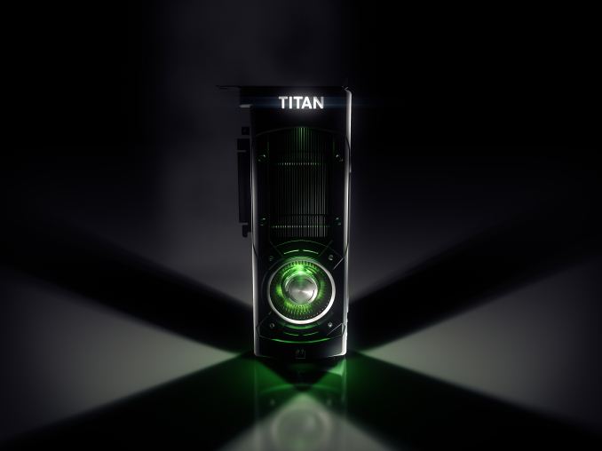
During today’s GDC session on Epic’s Unreal Engine, NVIDIA CEO Jen-Hsun Huang dropped in as a special guest to announce NVIDIA’s next high performance video card, the GeForce GTX Titan X.
In order to capitalize on the large audience of the Unreal session while not spoiling too much ahead of NVIDIA’s own event in 2 weeks – the NVIDIA GPU Technology Conference – NVIDIA is playing coy with details on the product, but they have released a handful of details along with a product image.
| NVIDIA Titan Specification Comparison | |||||
| GTX Titan X | GTX Titan Black | GTX Titan | |||
| Stream Processors | ? | 2880 | 2688 | ||
| Texture Units | ? | 240 | 224 | ||
| ROPs | 96? | 48 | 48 | ||
| Core Clock | ? | 889MHz | 837MHz | ||
| Boost Clock | ? | 980MHz | 876MHz | ||
| Memory Clock | ? | 7GHz GDDR5 | 6GHz GDDR5 | ||
| Memory Bus Width | 384-bit? | 384-bit | 384-bit | ||
| VRAM | 12GB | 6GB | 6GB | ||
| FP64 | ? | 1/3 FP32 | 1/3 FP32 | ||
| TDP | ? | 250W | 250W | ||
| Transistor Count | 8B | 7.1B | 7.1B | ||
| Architecture | Maxwell | Kepler | Kepler | ||
| Manufacturing Process | TSMC 28nm? | TSMC 28nm | TSMC 28nm | ||
| Launch Date | Soon | 2/18/14 | 02/21/13 | ||
| Launch Price | A Large Number | $999 | $999 | ||
The GPU underlying GTX Titan X is 8 billion transistors, which similar to the original GTX Titan’s launch means we’re almost certainly looking at Big Maxwell. NVIDIA will be pairing it with 12GB VRAM – indicating a 384-bit memory bus – and it will once again be using NVIDIA’s excellent metal cooler and shroud, originally introduced on the original GTX Titan.
No further details are being provided at this time, and we’re expecting to hear more about it at GTC. Meanwhile Epic’s master engine programmer Tim Sweeney was gifted the first GTX Titan X card, in recognition of NVIDIA and Epic’s long development partnership and the fact that Epic guys are always looking for more powerful video cards to push the envelope on Unreal Engine 4.


104 Comments
View All Comments
squatsh - Wednesday, March 4, 2015 - link
3072 Cuda cores*smartypnt4 - Wednesday, March 4, 2015 - link
I completely agree. These are the specs the leaks have pointed to as well.I'll also note this: this will be a 24-SMM design, with all SMMs on the die enabled, as 7.8B is around the upper limit of what TSMC can put on a single die right now at 28nm.
This means there won't be a new version of this chip like there was with the original Titan and Titan Black.
I also expect there to be a consumer version of this with 22 SMM's enabled, with the requisite ROPs and L2 cache disabled like they were on the 970 It'll likely also have 6GB of VRAM (For yes, 5GB of fast VRAM or however the math works out for their bus partitioning). This Titan Lite or 980 Ti or 985 or 990 or whatever they're gonna call it will be the real card to get for 4K from NVIDIA until they go through a process shrink. Two of those will be quite potent.
will54 - Wednesday, March 4, 2015 - link
actually if its a 384 bit bus it should be a full 6 GB'ssmartypnt4 - Wednesday, March 4, 2015 - link
The PCB will have 6GB, but it could be partitioned similarly to the 970's, which has a 3.5GB high-performance partition and a slow 512MB partition. I haven't worked out exactly what the equivalent would be based on SMM configuration, but it wouldn't surprise me to see 6GB on the PCB itself with something like a 768MB slow memory partition and 5.25GB fast memory partition.Or they'll do something totally new. No idea really. It's hard to even speculate what they might do. For the 22 SMM, it's conceivable they'll partition the memory like on the 970, but for the 20 SMM version, they could just disable one of the L2/ROP/Memory Controller units and go with a 320-bit bus for that part with 5GB of VRAM. That would actually be a really good part to have between the 980 and the other GM200-based cards.
Yojimbo - Wednesday, March 4, 2015 - link
This is a "prosumer" card which is sold with the idea that it could be used for things other than games, hence the FP64 at 1/3 FP32 for the other two Titan cards. It's very unlikely they would do such memory partitioning since, although 12GB is not going to be used for gaming, it might be used in other situations.squatsh - Wednesday, March 4, 2015 - link
The strange memory speeds in the 970 are due to the ROP set up now the SMMs, which can be completely independent. So you can have 22 SMMs and full speed memory. Overall the whole memorygate or whatever it is called was a bit of a mess, but as a technology the extra granularity is good for Nvidia (for yields) and us (they can be less conservative,ie 4gb of 3.5fast and .5 slo instead of just plain old 3gb). But I agree that while they are chopping off 2 SMMs for yields, they might mess around with the memory system again.squatsh - Wednesday, March 4, 2015 - link
(chopping off memory bits for the consumer lite version, if there will be one).Flunk - Wednesday, March 4, 2015 - link
I've been hoping for a 8GB 980TI and this leaves them room for that. They're going to have to do that if AMD brings out a 8GB 390x, which they probably will.hammer256 - Wednesday, March 4, 2015 - link
So is AMD going to use 20nm node for their GPUs? Or are they like Nvidia and sticking to the 28 until 16/14nm FFET?nevcairiel - Wednesday, March 4, 2015 - link
The 20nm process isn't good enough for high performance GPUs, so the consensus is that there won't be 20nm dGPUs, but they'll stick to 28nm for the time being and skip to FinFETs next.