The AMD Radeon R9 Fury X Review: Aiming For the Top
by Ryan Smith on July 2, 2015 11:15 AM ESTFiji’s Architecture: The Grandest of GCN 1.2
We’ll start off our in-depth look at the R9 Fury X with a look at the Fiji GPU underneath.
Like the Hawaii GPU before it, from a release standpoint Fiji is not really the pathfinder chip for its architecture, but rather it’s the largest version of it. Fiji itself is based on what we unofficially call Graphics Core Next 1.2 (aka GEN3), and ignoring HBM for the moment, Fiji incorporates a few smaller changes but otherwise remaining nearly identical to the previous GCN 1.2 chips. The pathfinder for GCN 1.2 in turn was Tonga, which was released back in September of 2014 as the Radeon R9 285.

So what does GCN 1.2 bring to the table over Hawaii and the other GCN 1.1 chips? Certainly the most well-known and marquee GCN 1.2 feature is AMD’s latest generation delta color compression technology. Tied in to Fiji’s ROPs, delta color compression augments AMD’s existing color compression capabilities with additional compression modes that are based around the patterns of pixels within a tile and the differences between them (i.e. the delta), increasing how frequently and by how much frame buffers (and RTs) can be compressed.
Frame buffer operations are among the most bandwidth intensive in a GPU – it’s a lot of pixels that need to be resolved and written to a buffer – so reducing the amount of memory bandwidth these operations draw on can significantly increase the effective memory bandwidth of a GPU. In AMD’s case, GCN 1.2’s delta color compression improvements are designed to deliver up to a 40% increase in memory bandwidth efficiency, with individual tiles being compressible at up to an 8:1 ratio. Overall, while the lossless nature of this compression means that the exact amount of compression taking place changes frame by frame, tile by tile, it is at the end of the day one of the most significant improvements to GCN 1.2. For Radeon R9 285 it allowed AMD to deliver similar memory performance on a 256-bit memory bus (33% smaller than R9 280’s), and for Fiji it goes hand-in-hand with HBM to give Fiji an immense amount of effective memory bandwidth to play with.
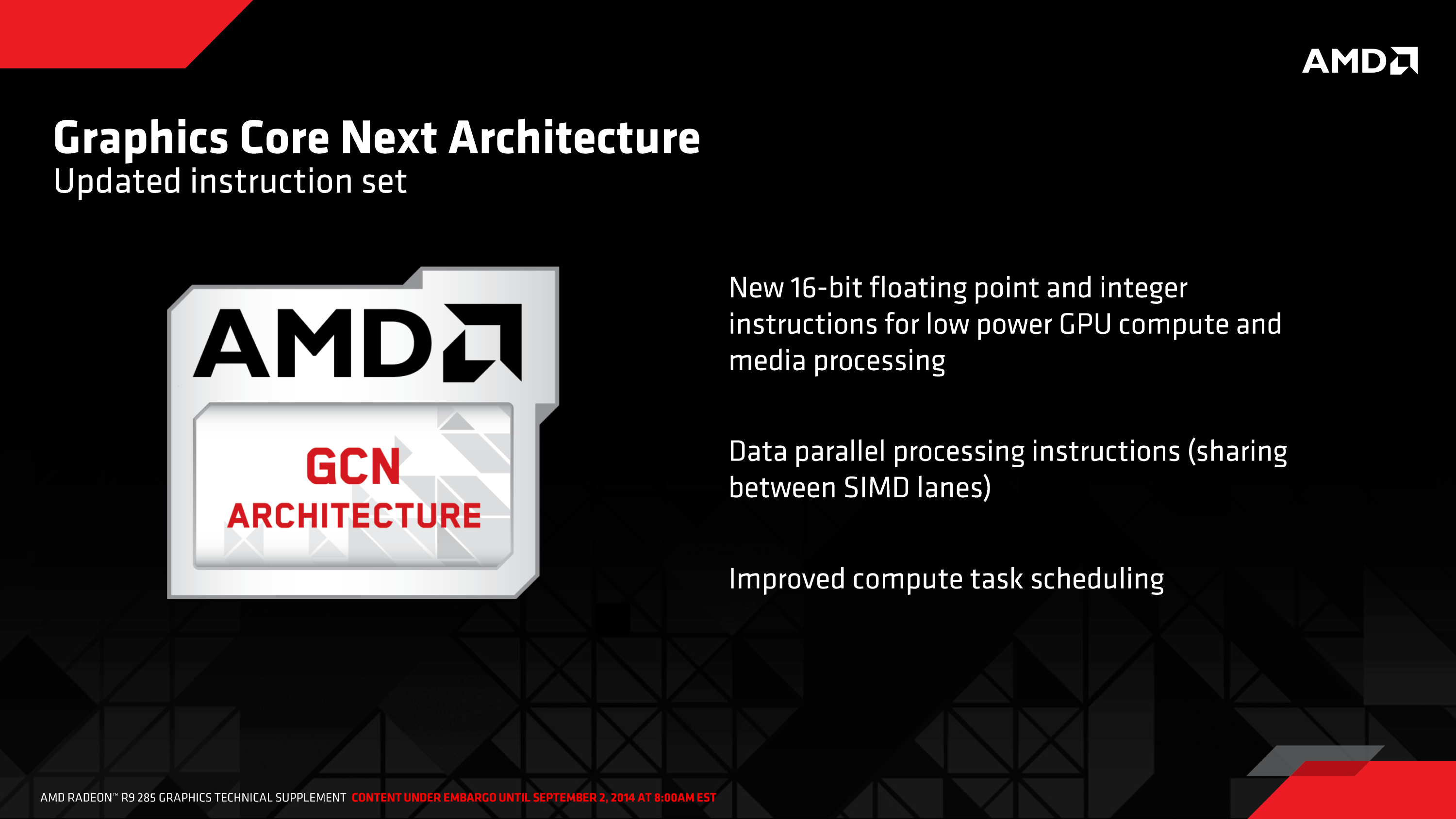
Moving on, AMD has also made some changes under the hood at the ALU/shader level for GCN 1.2. Many of these changes are primarily for AMD’s Carrizo APU, where task scheduling improvements go hand-in-hand with the AMD’s Heterogeneous System Architecture initiative and deliver improvements to allow the CPU and GPU to more easily deliver work to each other. Similarly, 16-bit instructions are intended to save on power consumption in mobile devices that use lower precision math for basic rendering.

More applicable to Fiji and its derivatives are the improvements to data-parallel processing. GCN 1.2 now has the ability for data to be shared between SIMD lanes in a limited fashion, beyond existing swizzling and other data organizations methods. This is one of those low-level tweaks I’m actually a bit surprised AMD even mentioned (though I’m glad they did) as it’s a little tweak that’s going to be very algorithm specific. For non-programmers there’s not much to see, but for programmers – particularly OpenCL programmers – this will enable newer, more efficient algorithms where when the nature of the work requires working with data in adjacent lanes.
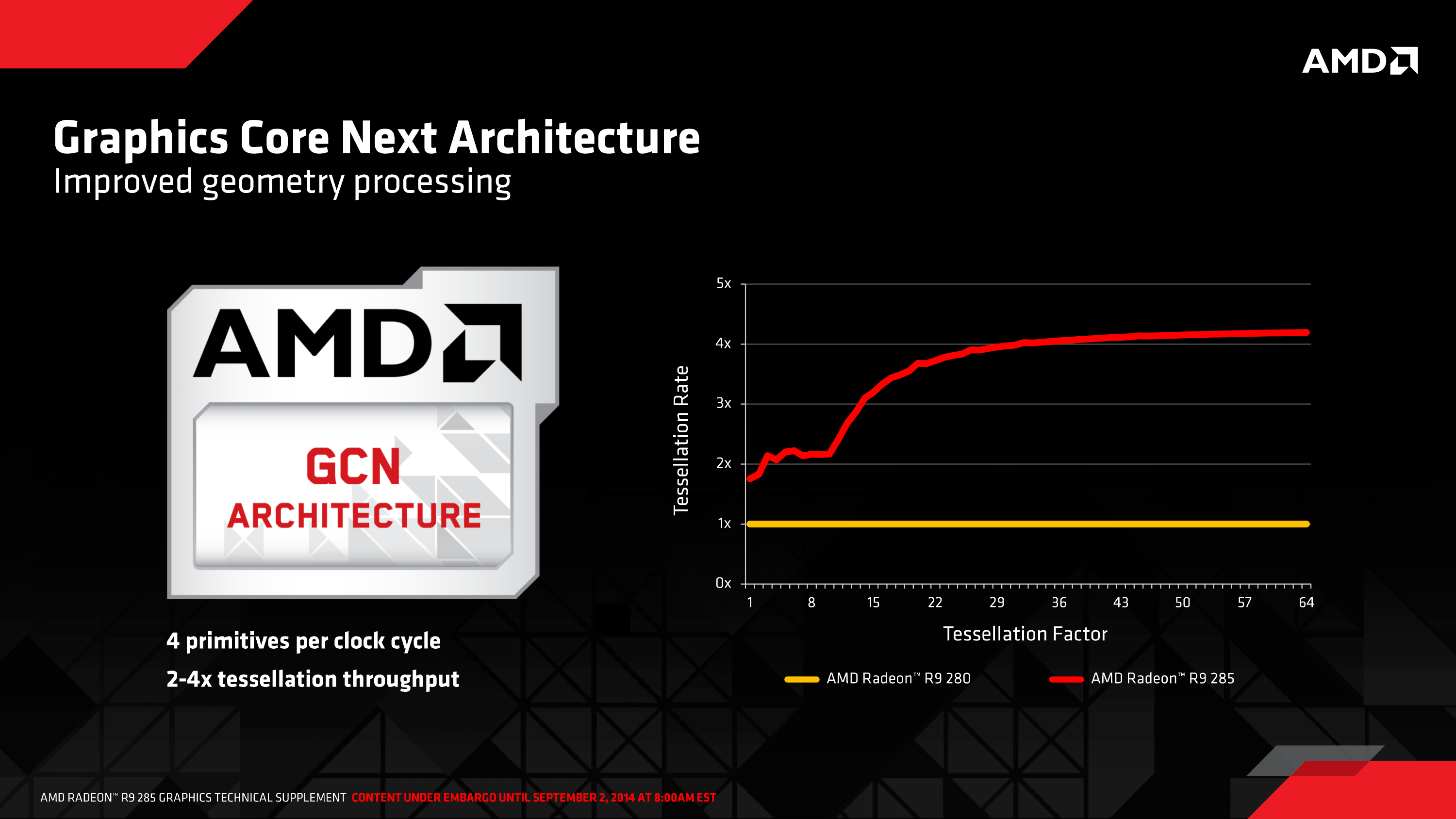
But for gamers, perhaps the most significant architectural improvement to GCN 1.2 and thereby Fiji are the changes made to tessellation and geometry processing. There is no single silver bullet here – after going with a 4-wide geometry front-end in Hawaii, AMD hasn’t changed it for Tonga or Fiji – but AMD has put in quite a bit of effort in to improving how geometry data moves around within the chip and how it’s used, on the basis that at this point the limitations aren’t in raw geometry performance, but rather the difficulties in achieving that performance.
Much of this effort has been invested in better handling small geometry, whether it’s large quantities of small batches, or even small quantities of small batches. The inclusion of small instance caching, for example, allows the GPU to better keep small batches of draw calls in cache, allowing them to be referenced and/or reused in the future without having to go to off-cache memory. Similarly, AMD can now store certain cases of vertex inputs for the geometry shader in shared memory, which like small instance caching allows for processing to take place more frequently on-chip, improving performance and cutting down on DRAM traffic.
More specific to Fiji’s incarnation of GCN is how distribution is handled. Load balancing and distribution among the geometry frontends is improved overall, including some low-level optimizations to how primitives generated from tessellation are distributed. Generally speaking distribution is a means to improve performance by removing bottlenecks, however AMD is now catching a specific edge case where small amplification factors don’t generate a lot of primitives, and in those cases they’re now skipping distribution since the gains are minimal, and more likely than not the cost from the bus traffic is greater than the benefits of distribution.
Finally, AMD has also expanded the vertex reuse window on GCN 1.2. As in the general case of reuse windows, the vertex reuse window is a cache of sorts for vertex data, allowing old results to be held in waiting in case they are needed again (as is often the cases in graphics). Though they aren’t telling us just how large the window now is, GCN 1.2 now features a larger window, which increases the hit rate for vertex data and as a result further edges geometry performance up since that data no longer needs to be regenerated.
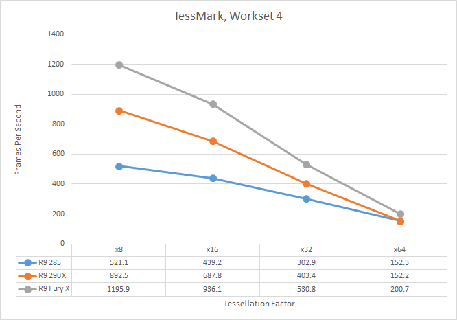
As with our R9 285 review, I took the time to quickly run TessMark across the x8/x16/x32/x64 tessellation factors just to see how tessellation and geometry performance scales on AMD’s cards as the tessellation factor increases. Keeping in mind that all of the parts here have a 4-wide geometry front-end, the R9 285, R9 290X, and R9 Fury X all have the same geometry throughput on paper, give or take 10% for clockspeeds. What we find is that Fury X shows significant performance improvements at all levels, beating not only the Hawaii based R9 290X, but even the Tonga based R9 285. Tessellation performance is consistently 33% ahead of the R9 290X, while against Tonga it’s anywhere between a 33% lead at high factors to a 130% lead at low tessellation factors, showing the influence of AMD’s changes to how tessellation is handled with low factors.


458 Comments
View All Comments
just4U - Saturday, July 4, 2015 - link
I thought it was great as well.. It had a lot more meat to it then I was expecting. Ryan might have been late to the party but he's getting more feedback than most other sites on his review so that shows that it was highly anticipated.B3an - Saturday, July 4, 2015 - link
I don't understand why the Fury X doesn't perform better... It's specs are considerably better than a 290X/390X and it's memory bandwidth is far higher than any other card out there... yet it still can't beat the 980 Ti and should also be faster than it already is compared to the 290X. It just doesn't make sense.just4U - Saturday, July 4, 2015 - link
Early drivers and perhaps the change over into a new form of memory tech has a bit of a tech curve that isn't fully realized yet.Oxford Guy - Saturday, July 4, 2015 - link
Perhaps DX11 is holding it back. As far as I understand it, Maxwell is more optimized for DX11 than AMD's cards are. AMD really should have sponsored a game engine or something so that there would have been a DX12 title available for benchmarkers with this card's launch.dominopourous - Saturday, July 4, 2015 - link
Great stuff. Can we get a benchmarks with these cards overclocked? I'm thinking the 980 Ti and the Titan X will scale much better with overclocking compared to Fury X.Mark_gb - Saturday, July 4, 2015 - link
Great review. With 1 exception.Once again, the 400 AMP number is tossed around as how much power the Fury X can handle. But think about that for one second. Even a EVGA SuperNOVA 1600 G2 Power Supply is extreme overkill for a system with a single Fury X in it, and its +12V rail only provides 133.3 amps.
That 400 AMP number is wrong. Very wrong. It should be 400 watts. Push 400 Amps into a Fury X and it most likely would literally explode. I would not want to be anywhere near that event.
AngelOfTheAbyss - Saturday, July 4, 2015 - link
The operating voltage of the Fury chip is probably around 1V, so 400A sounds correct (1V*400A = 400W).meacupla - Saturday, July 4, 2015 - link
okay, see, it's not 12V * 400A = 4800W. It's 1V (or around 1V) * 400A = 400W4800W would trip most 115VAC circuit breakers, as that would be 41A on 115VAC, before you even start accounting for conversion losses.
bugsy1339 - Saturday, July 4, 2015 - link
Anyone hear about Nvidia lowering thier graphics quality to get a higher frame rate in reviews vs Fury? Reference is semi accurate forum 7/3 (Nvidia reduces IQ to boost performance on 980TI? )sa365 - Sunday, July 5, 2015 - link
I too would like to know more re:bugsy1939 comment.Have Nvidia been caught out with lower IQ levels forced in the driver?