AMD Launches the A8-7670K: Filling in the Gaps
by Ian Cutress on July 20, 2015 5:40 PM EST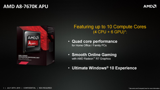
AMD and Intel, in the last few years, have taken different approaches to how many CPUs enter the mainstream line of the market. Intel has historically had a large product stack, with processors at almost every frequency varying by 100 MHz and slowly rising in core count as well as cache and integrated graphics. AMD’s approach on the other hand is to release a handful of new models every quarter, initially covering the bases on day one and slowing updating the mid points (as well as new high end models) as a lithography node improves in yield and performance and the design matures. We recently took a look at the last launch, the AMD A10-7870K, as well as one at the beginning of the year in the shape of the A8-7650K. The A10-7870K was the first in a line known as the Kaveri Refresh models, or as per AMD’s internal codename ‘Godavari’. The A8-7670K is the second iteration of this line.
The Kaveri Refresh line, or so we are told, is a result of an improved production methodology for better frequency/voltage characteristics and better binning. In the case of the A10-7870K, we were told that the CPU has a minor +0.05 volt increase in the average stock voltage to account for the extra frequency, but due to the improvements the TDP remained the same (95W). In this circumstance, AMD improves on the A8-7650K with an extra 300 MHz to the base frequency (usually the main TDP killer) and an extra 100 MHz on the turbo. This is combined with a 37 MHz increase in the graphics side of the equation, again within the same TDP.
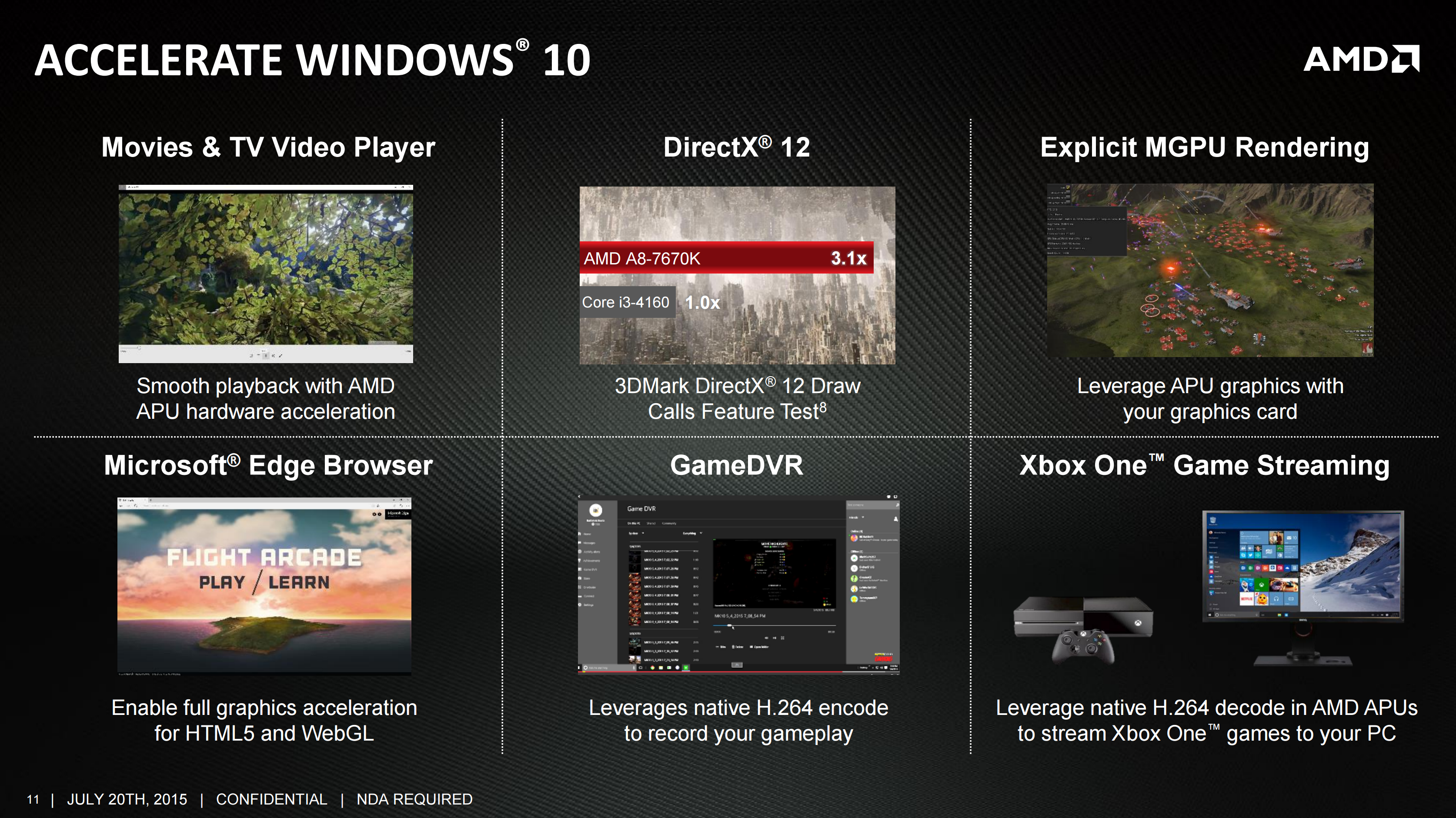
We covered a lot in the A10-7870K review which also applies here to the A8-7670K, although the A8 follows the other A8 APUs by having six compute units for the graphics, or 384 SPs. As AMD does not have a new mainstream desktop APU launch for Windows 10, the current stack of Kaveri and Kaveri Refresh APUs are going to be the focus for AMD, especially with back-to-school sales late in the summer. As a result, a good portion of the press release for the A8-7670K revolves around the use of AMD’s GCN architecture and its alignment to AMD’s mainstream graphics cards, allowing any software that is accelerated by one to be accelerated by the other. As shown above, this includes video playback, DirectX 12, accelerated video encoding and streaming as well.
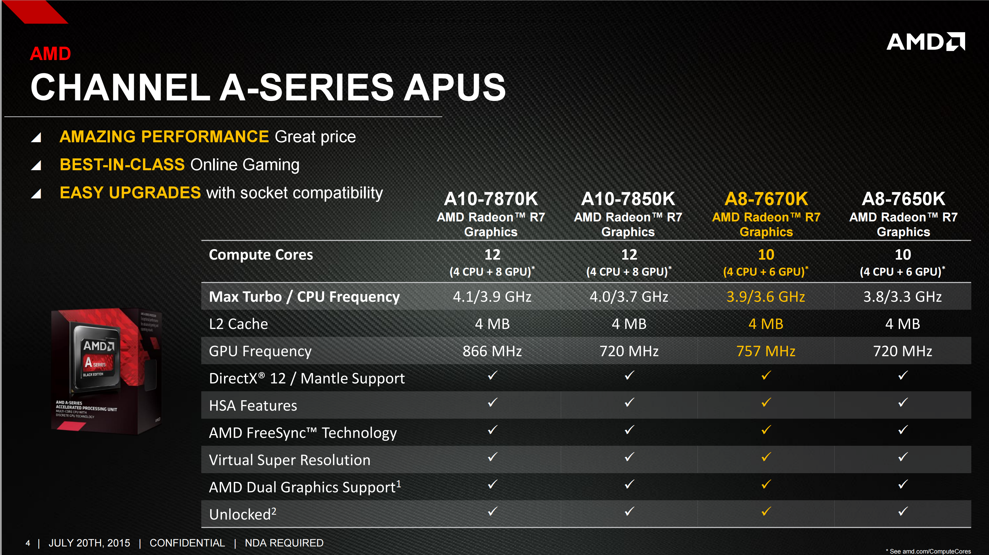
| AMD Kaveri Lineup | ||||||||
| A10- 7870K |
A10- 7850K |
A10- 7800 |
A10- 7700K |
A8- 7670K |
A8- 7650K |
A8- 7600 |
X4 860K |
|
| Price | $137 | $134 | $131 | $120 | $118 | $104 | $89 | $85 |
| Modules | 2 | 2 | 2 | 2 | 2 | 2 | 2 | 2 |
| Threads | 4 | 4 | 4 | 4 | 4 | 4 | 4 | 4 |
| Core Freq. (GHz) | 3.9-4.1 | 3.7-4.0 | 3.5-3.9 | 3.4-3.8 | 3.6-3.9 | 3.3-3.8 | 3.1-3.8 | 3.7-4.0 |
| Compute Units | 4+8 | 4+8 | 4+8 | 4+6 | 4+6 | 4+6 | 4+6 | 4+0 |
| Streaming Processors |
512 | 512 | 512 | 384 | 384 | 384 | 384 | N/A |
| IGP Freq. (MHz) | 866 | 720 | 720 | 720 | 754 | 720 | 720 | N/A |
| TDP | 95W | 95W | 65W | 95W | 95W | 95W | 65W | 95W |
| DRAM Frequency |
2133 | 2133 | 2133 | 2133 | 2133 | 2133 | 2133 | 1866 |
| L2 Cache | 2x2MB | 2x2MB | 2x2MB | 2x2MB | 2x2MB | 2x2MB | 2x2MB | 2x2MB |
AMD’s marketing slides position the A8-7670K at $118 MSRP against the i3-4160 at $120 – and as a result we see benchmarks that require four full INT cores (7-zip), or those that rely on the GPU for part of their compute (PCMark 8), coming ahead. When compared to a discrete GPU solution, AMD suggests that an equivalent cost to the A8 is an Intel Pentium G3258 with a GT 730 discrete card, where the discrete card loses in popular eSports gaming titles. As has been the case for AMD, they play to the strengths of their product, and these lie in that sub-$700 gaming PC (based on the A68H platform) built for eSports that should also help with future DirectX 12 multi-GPU rendered titles.

The AMD A8-7670K is officially launched today and currently retails at $110 on Newegg, making it cheaper than the official MSRP. If we get a sample in, we’ll write a review and add the data to our processor comparison database Bench.
Source: AMD


33 Comments
View All Comments
looncraz - Tuesday, July 21, 2015 - link
HBM on an APU would almost certainly just use a 1024-bit bus, which would provide 128-256GB/s of bandwidth - which is astonishing. However, it would be very difficult to use it as system RAM. I'd expect a 1 or 2GB HBM capacity, with possibly some acting as an L4 cache - but not likely in the first iteration.yankeeDDL - Tuesday, July 21, 2015 - link
I really hope that you’re wrong. Yes, the interposer is expensive, and no, I really don’t think we can get an APU with HBP for ~$110, but, hopefully, the technology for Fury can scale a bit and give us an APU with 1GB of HBM, is going to push the performance up one notch without needing any architectural improvement.Just look at how the Iris Pro on the Intel’s parts: without on-chip Dram they get creamed. Add the eDram and they fly (granted that the GPU is not identical, but the “jump” is huge).
The issue with Intel’s solution is that it is insanely pricey ($300+), and make little sense, so it’s key to have HBM at ~$200 price point: that should blow the entry level discrete GPU out of the market.
psychobriggsy - Tuesday, July 21, 2015 - link
If Zen is good, and competitive with Intel, then AMD can start selling $300+ APUs again, using HBM2 to accelerate the integrated graphics (which should be 1024 shaders at least on 14nm).There will be a SKU that solely uses HBM (for ultra portables), probably with 8GB on board. There may be a SKU that also has DDR4 for expansion, and that uses a portion of the HBM as a massive cache.
psychobriggsy - Tuesday, July 21, 2015 - link
The interposer for an APU would be a lot smaller than the one for Fiji - Fiji is 600mm^2! They are also quite cheap compared to logic - they use an old proven process with few layers.AMD will move to using an interposer when it releases a Zen based APU, maybe late 2016 or 2017. Their current APUs don't have HBM memory controllers on board. I do wonder what their mid-2016 plan is in the APU area.
beginner99 - Tuesday, July 21, 2015 - link
The interposer cost single digits $. It's made on an old process (65nm for Fiji GPU) and you can omit the most costly steps that need to be done when creating a real processor.Shadow7037932 - Monday, July 20, 2015 - link
Not any time soon. Probably a generation or so out before the midrange and up GPU lineup gets the HBM treatment, followed by the APUs. However, it'szodiacfml - Tuesday, July 21, 2015 - link
Too expensive. Imagine, it is more expensive than GDDR5. Maybe we will see HBM on APUs once their GPUs uses HBM2.ShieTar - Tuesday, July 21, 2015 - link
AMD could have gone for a Quad-Channel-FM Plattform (they have quad-channel opterons), or switched to DDR4 early. They don't seem very motivated to significantly improve the APU-Performance right now, rather just looking to collect their money from people with small budgets.Nagorak - Tuesday, July 21, 2015 - link
Switching to DDR 4 early would have been about the stupidest thing they could have done. Right now they are competing as a budget alternative to Intel. Having to buy memory that costs twice as much, or more, would not have helped them at all.meacupla - Monday, August 3, 2015 - link
What is the point of reducing the GPU memory bottleneck, when the CPU computing portion is lacking in the first place?Also, quad channel memory is going to increase the cost severely and you are very likely to end up with a massive 2000pin+ socket and, by association, massive mobos as well.
HBM is just a better design that can be applied to both GPU and APU.