
Original Link: https://www.anandtech.com/show/248
| In the past, the trend of innovation has primarily been towards bigger and better solutions for the market. Ranging from bigger and more powerful computers to bigger and more powerful storage devices, the PC hardware industry has kept up its tendency to enforce the "bigger is better" policy human nature tends to generally abide by. With Intel virtually controlling the entire chipset industry as the chief supplier of chipset core logic for motherboards, the past two years have definitely been hard times for the competing manufacturers in the industry, now cut down to three major competitors: Acer Labs Incorporated, Silicon Integrated Systems, and VIA Technologies. | 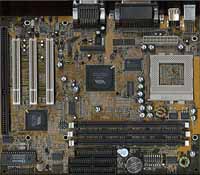 |
| These three chipset manufacturers were the select few that made it through the chipset industry's version of Darwinism, or survival of the fittest. For those of you that weren't in the market for a motherboard a few years back, names like Opti and VLSI dominated most of the third party chipset sales. It wasn't until the arguably premature demise of the 486 and the unexpected move towards the Pentium architecture that the seemingly endless list of chipset manufacturers was cut down to less than a handful. | |
Among those remaining four, Intel took the lead, and far behind the microprocessor giant lay the foundation of a company that was not ready for the market they were destined to take upon their shoulders, this company is none other than VIA Technologies.
The three lettered chipset manufacturer quickly began to gain weight in the chipset industry during the days of the Intel 430TX chipset, a product whose flaws left many users desiring more. VIA saw a golden opportunity with the Socket-7 interface at the time and the flaws in Intel's flagship 430TX (as well as their 430FX and 430HX products) chipset and chose to exploit them by producing a solution that was clearly superior to Intel's product line in virtually every way. Although the original success of the non-Intel chipsets in the Socket-7 market was limited, it eventually grew to a hefty proportion, and with Intel's abandonment of the Socket-7 platform in favor of their proprietary Slot-1 (Pentium II) interface, VIA was left with a tremendous burden: breathing life into a quickly dying Socket-7 standard.
Luckily, another "three lettered" manufacturer saw the same golden opportunity VIA envisioned, and they took it upon themselves to help drive the Socket-7 industry into direct competition with Intel's Slot-1 creations by modifying the Socket-7 chipset specification dramatically. That company turned out to be Advanced Micro Devices, the pioneers of the "Super7" standard, or AMD for short.
With AMD providing the driving force (even more importantly, the processors) to support an extension of the Socket-7 interface standard (Super7) and VIA providing the support on the chipset side of things, the combination of the two forces would almost certainly spell trouble for Intel. Unfortunately, a lack of support from motherboard manufacturers during the critical public developmental stages of AMD's and VIA's cooperative efforts left Intel with a smirk on their faces, and AMD/VIA at a loss with nothing more than a slim chance at proving themselves. At the high end, it seemed like their new "Super7" concoction would never even receive the time of day from any potential buyers. This was simply because a large percentage of those that wanted a high end solution were normally willing to pay the extra premium for a household name they all knew and trusted (how many AMD commercials have you seen on TV?). If anything, the continuing trend of buying Intel proved the statement that money does make the world go 'round, meaning that the business world does revolve around money and making a profit, simple, no?
Ironically enough, the solution to the problems AMD and VIA faced was placed directly beneath their noses, instead of going after the small percentage of those that would even consider a non-Intel system for a high end solution, why not concentrate on the more mainstream market? Those that couldn't afford Intel's high prices would finally be given a chance to have a shot at a more than decent computer, without paying that premium; and above all, the percentage of the market that once had to settle for second or third generation "hand-down" products could now taste the performance of a system that could rival the more expensive bad boys, all for a cost often under $1000.
Building the sub $1000 PC
The key to building the sub $1000 PC turned out to be in the integration of the components that go into a computer, while the technology has been around for years allowing manufacturers to integrate sound and video onto a motherboard, the ability to do so and achieve a fairly competitive system by the standards of the day was somewhat limited. Motherboard manufacturers have taken it upon themselves to provide the component integration into their products, by including low cost 3D accelerators and cheap audio controllers on their boards, however the success of these products is reaching a maximum as there is only so much a motherboard manufacturer can do with a single chipset design.
Leave it to VIA to rescue (although not as dramatically as that) the industry once again, providing the market with a true, low-cost, highly integrated, chipset solution that would require very little modification of the current motherboard design in order to implement it. Imagine a motherboard, with on-board video, sound, and even an on-board modem controller; now imagine that all of those features were integrated into two chips, along side the normal functions of a motherboard. What you're imagining is VIA's latest production, the MVP4 chipset, not so much a successor, rather a compliment to their already successful MVP3 chipset.
MVP4 Specifications
As taken from www.via.com.tw:
The Apollo MVP4 is an advanced System Multimedia Architecture (SMA) PC core logic chipset for Super 7 PC systems. The VIA Apollo MVP4 is a combination of the widely successful VIA Apollo MVP3 and a high performance 2D/3D graphics controller. Paired with the new VIA VT82C686 Super South bridge, The MVP4 is a compelling solution for cost-effective, full-feature desktop and mobile PC designs.
The MVP4 integrates an AGP 2.0 - compliant 2D/3D AGP graphics controller into the north bridge of the chipset. Packed with features, the controller incorporates a 64-bit 2D/3D graphics engine and video accelerator with advanced DVD video and optional TV output capability. The controller supports Win-95 and Win-98 / NT5 miniport drivers.
For full feature system designs, the Apollo MVP4 is paired with the VIA VT82C686 south bridge. Highly advanced, the south bridge combines an integrated 2D/3D engine with DVD hardware acceleration, AC-97 audio support for SoundBlaster Pro and FM synthesis legacy audio, super I/O, and hardware monitoring capabilities.
Features
-
VT82C501 SMA North Bridge
- Integrated advanced 2D/3D AGP graphics with setup engine and DVD hardware acceleration
- 100MHz front side / memory bus
- Advanced ECC memory controller supports up to 768MB PC100 SDRAM, Virtual Channel SDRAM, EDO, FP
- Compatible with all Socket 7 processors
- Synchronous/Asynchronous AGP/PCI/memory operation
- 66/75/83/95/100MHz FSB capabilities
- 492-pin BGA package
- VT82C686 Super South Bridge
- Integrated AC-97 2.0 (meets PC98 (TM) Basic Audio spec.) / SoundBlaster-compatible legacy audio
- Integrated Super I/O: FDC, parallel port, serial port, IR
- Voltage, temperature, and fan speed hardware monitoring
- UDMA/33 / ATA-66
- Advanced mobile PC power management
- Supports ATAPI compliant devices including DVD devices
- USB
- ACPI
- Compatible with all VIA Socket 7 and Slot 1 north bridges
- 352-pin BGA package
At first Sight
At first sight, the MVP4 can be a relatively frightening product, simply because the thought of having an AGP accelerator integrated into the North Bridge of a chipset is quite limiting. This is completely true, meaning that the MVP4 will not be a high end solution for those users looking to achieve the best possible performance out of their systems with no consideration for cost. The MVP4 will, however, be a solution that is both cost effective, and a good performer for the cost. For direct competition against Intel's Pentium III, you'll still want to stick to the MVP3/K6-3 combo, however for a more cost effective solution that would be an excellent competitor to Intel's dominant Celeron line of systems, the MVP4 will definitely make its presence well known.
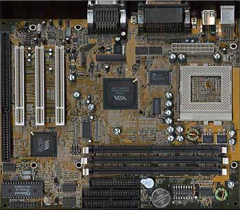
In terms of chipset performance, the MVP4 is no more and no less than the MVP3, the performance issues begin to factor in when you take into account the speed of the integrated hardware, such as the integrated Trident Blade 3D video controller. The key improvements the MVP4 holds over the MVP3 revolve around, as you may be able to guess, a more all-in-one design, being highly integrated, and low in cost.
The North Bridge
| The VT82C501 System Multimedia Architecture (SMA) North Bridge controller that makes up half of the MVP4 chipset is home to the same features the MVP3's North Bridge (VT82C598) controller, with the addition of two healthy and welcome enhancements. The heart of the North Bridge controller, as the acronym SMA alludes to, is the addition of an integrated multimedia video device that supports 2D/3D and hardware DVD acceleration. The integrated AGP video solution was custom manufactured for VIA by a fairly well known company in the PC video industry, Trident. | 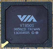 |
Although they're not famous for making the most high performance graphics accelerators and chipsets, Trident managed to come through quite well with the integrated Blade 3D core present on the VT82C501 North Bridge. In a recent communication with Trident about the company's goals for the Blade 3D core, AnandTech was told plainly and simply that the Blade 3D does not compete with the 3Dfx and nVidia's of the world, however the price to performance ratio the Blade 3D offers is quite impressive.
While it would have been ideal, for gamers at least, for VIA to have picked something along the lines of a TNT to integrate into the MVP4, from a cost perspective, Trident's name and their product made the perfect finish to VIA's low-cost flagship. You can't expect the performance of the integrated Trident core to be top notch, however as AnandTech's tests of the MVP4 showed, the integration of the core into the physical chipset allowed for much higher bus transfer tests in the raw 2D and 3D performance comparisons that were conducted.
Since the video controller is present at the lowest of levels (physically integrated into the North Bridge controller), communication between the video and memory subsystems it at a peak in efficiency as the video bus is not being limited by the specifications of an external interface. As far as memory is concerned, the integrated video controller shares the system memory using up to 8MB as its frame buffer memory (as was the case with the board AnandTech received), a decent sized frame buffer which should be large enough for the applications, both business and entertainment related, that the MVP4 may be pitted up against.
The North Bridge also allows for an integrated hardware DVD decoder, a feature that not only eliminates the need for an external PCI DVD decoder (therefore occupying one of the limited PCI slots on a low-cost/low-expansion MVP4 board) but it also brings high quality and high performance DVD playback into the hands of the masses. A quick search with most on-line vendors will reveal that a generic IDE DVD drive will set you back no more than $100 for a decent drive, often times dipping down into the $70 level, which definitely helps push the growing DVD standard into the hands of more users, in more homes at a more affordable price.
On the memory side of things, the MVP4 North Bridge supports a maximum of 2048KB (2MB) of Level 2 cache, and is capable of caching up to 508MB of memory although the theoretical maximum installed memory limitation of the chipset is 768MB. The 508MB cacheable memory area is achieved with a 2MB L2 cache size, with 1MB boards offering a 254MB cacheable memory area, and 512KB L2 boards providing a 127MB cacheable memory area. Although this is a definite downside to the MVP4 and the Super7 platform in general, if you find yourself requiring more than 254/508MB of system RAM you'll want to drop any thoughts of a cost efficient system right away.
For those of you that are not familiar with the term cacheable memory area, if you were to physically exceed your motherboard/chipset's cacheable memory area (i.e. installing 768MB of RAM in a 2MB L2 MVP4 board), any memory accesses made above the cacheable memory limit (i.e. 508MB w/ 2MB of L2 on a MVP4) would be effectively slower than those beneath the limit, degrading your overall system performance.
The Super South Bridge
| A fitting name for a deserving product, the second part to the MVP4 equation is the VT82C686 Super South Bridge controller. The South Bridge has generally been the home to the PCI Hard Disk controller and other such I/O related functions, and in an extension of tradition, VIA has taken the standard South Bridge one step further with their Super South Bridge present as a part of the MVP4 chipset. | 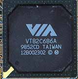 |
Starting with its primary function, the Super South Bridge contains the same Ultra DMA/33 PCI EIDE Bus Master controller that the MVP3's South Bridge features with a new twist, support for the new Ultra ATA-66 standard. As you all are probably already aware of, the maximum theoretical transfer rate on an Ultra ATA-33 hard disk is, as the name implies, 33.3MB/s. The Ultra ATA-66 standard doubles that maximum theoretical burst transfer rate to 66.6MB/s while increasing the cable specifications to call for a 40-pin/80-conductor cable (as opposed to the standard 40-pin/40-conductor cables) to improve data integrity during high speed data transfers. For a more in-depth description of Ultra ATA-66, read Western Digital's Overview of the Standard.
At the time of publication, AnandTech did not have the opportunity to benchmark an Ultra ATA-66 vs Ultra ATA-33 comparison, however VIA has an updated set of Bus Master drivers with official Ultra ATA-66 support in the works, so rest assured that AnandTech will bring you a full fledged comparison as soon as the drivers are ready.
Leaving hard disk controllers behind, the Super South Bridge adds another unique feature to the already extensive support list, USB2. Towards the end of 1998, a few motherboards began popping up that had support for front USB ports, unfortunately using a USB port on the front of your case would require that one be taken off of the back of your case. The addition of USB2 allows for an additional 2 ports to be supported on the motherboard itself, bringing the total supported USB ports to 4 ports (ideally, 2 front and 2 back), and with each port supporting a theoretical maximum of 127 devices, that's a total of 508 devices. Chances are you'll never come close to reaching that limit (there aren't enough USB devices in existence to reach that limit), but it's better to be safe with an unreasonable limit than to begin finding ways to cut down on USB devices.
In spite of VIA's extensive work on an integrated IEEE1394 solution (Firewire), the up and coming standard failed to make it into the Super South Bridge of the MVP4. When AnandTech asked about the possibility of including Firewire in a later revision of the chipset VIA indicated that if the technology were integrated into the South Bridge controller, a relatively smooth integration could be performed by simply replacing the South Bridge chip with an updated release including 1394 support. It seems like only time will tell, but don't be too surprised if the second half of 1999 holds 1394 integration with some of VIA's chipsets.
Why call the VT82C686 controller a Super South Bridge controller? For no reason other than the integrated audio and modem CODECs that the Super South Bridge controller houses, allowing for extremely cost effective integration of on-board sound and modem connections with the possibility of integrated Ethernet controllers in the future if the demand is present. Once again, the modification of a South Bridge controller is hardly anything in comparison to a change in the North Bridge controller, simply because the South Bridge does not interact with any of the memory or video buses, leaving the South Bridge as a very flexible part of VIA's chipset solution.
| In order to help cut costs even more, Intel's AMR (Audio/Modem Riser) specification is used in interfacing with the on-board audio/modem CODECs. By using an external riser specification, a motherboard manufacturer does not have to wait for FCC certification for an integrated modem or audio controller in order to move on with production of the motherboard as the FCC certification can be more easily performed on the individual components rather than on a highly integrated motherboard. | 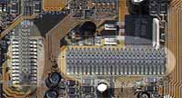 |
Although AMR integration does not border on the bleeding edge of technology in comparison to stand alone modem and sound solutions, the specification does set a baseline standard for audio and modem integration while cutting costs at the same time.
Performance Conclusion
- AMD K6-2 300 (3DNow! support was disabled)
- FIC PA-2013 w/ 1MB L2 Cache (MVP3), Prototype MVP4 board w/ 1MB L2 Cache
- 128MB PC100 SDRAM
- Western Digital Caviar AC35100 - UltraATA
- Canopus Spectra 2500 TNT AGP Video Card (16MB - MVP3 benchmarks)
- Integrated Trident Blade 3D (8MB - MVP4 benchmarks)
All Winstone tests were run at 1024 x 768 x 16 bit color
All Final Reality tests were conducted at 1024 x 768 x
16-bit color and were run using version Final
Reality 1.01
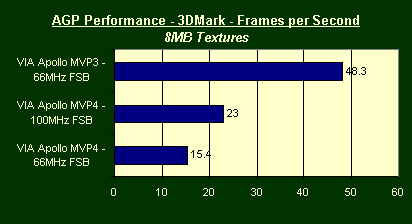
All 3Dmark tests were conducted at 800 x 600 x 32-bit color, triple buffered, using 16 bit Z-buffering
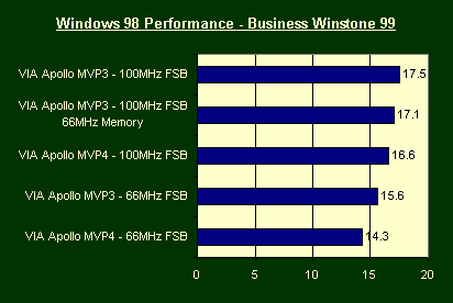
As you can tell, the business performance of the MVP4 chipset is virtually identical to that of the MVP3, the only difference being that the slower Trident video core present on the MVP4 is no match for the TNT used in the MVP3 test system. Likewise, the price of the MVP3 system outfitted with a TNT card is no match for the price of the MVP4 system, with the only performance difference from a business perspective being a few percent in favor of the MVP3. How much is 5% worth to you?
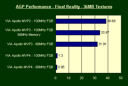
Here's the perfect illustration of why the MVP4 is not a gamer's solution, the Trident core is simply not a full AGP implementation, meaning that once its frame buffer is exceeded (in this case, 8MB) there is a significant drop in performance as there is a considerable amount of texture swapping to and from the system memory, an extremely slow route, even for a video accelerator that is integrated into the chipset on a motherboard.
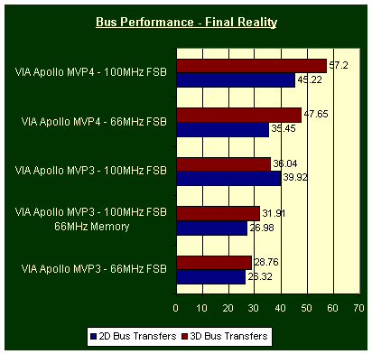
The raw performance across the video bus illustrates the advantages having an integrated video core provides the end user with, unfortunately the relatively weak core performance of the Trident accelerator will keep the high bus performance from truly being noticed. For everyone else but gamers, the MVP4 is an incredible strong solution, especially when considering its price to performance ratio. Do remember that the MVP4 system is being compared to a much more expensive TNT based MVP3 system, a world of difference if you're constructing a low-cost PC.

Where to expect MVP4 based motherboards
You can pretty much expect most MVP4 boards to be offered in the most cost effective manner, meaning that 9 out of every 10 MVP4 boards will be built on a Micro ATX PCB, once again in an attempt to keep costs low. Motherboard manufacturers such as FIC already have MVP4 designs in the works, and in combination with the soon to come K6-2 price cuts and the release of AMD's K6-3, the MVP4 should make for an interesting low-cost/high-performance alternative to Intel's already dominant Celeron-BX/ZX knockout. 1999 has started out, as we could all pretty much predict back in 1998, as a year of competition, and what we're seeing is that competition unfold before our eyes. If anything, the market is being pushed towards more cost effective solutions, while refraining from sacrificing performance. Has VIA accomplished that with the MVP4? Absolutely, however will the product be a success? That's up to the market to decide.


