Original Link: https://www.anandtech.com/show/4008/nvidias-geforce-gtx-580
NVIDIA's GeForce GTX 580: Fermi Refined
by Ryan Smith on November 9, 2010 9:00 AM ESTThe GTX 480… it’s hotter, it’s noisier, and it’s more power hungry, all for 10-15% more performance. If you need the fastest thing you can get then the choice is clear, otherwise you’ll have some thinking to decide what you want and what you’re willing to live with in return.
The GeForce GTX 480 and the associated GF100 GPU have presented us with an interesting situation over the last year. On the one hand NVIDIA reclaimed their crown for the fastest single GPU card on the market, and in time used the same GPU to give rise to a new breed of HPC cards that have significantly expanded the capabilities of GPU computing. On the other hand, like a worn and weary athlete finally crossing the finish line, this didn’t come easy for NVIDIA. GF100 was late, and the GTX 480 while fast was still hot & loud for what it was.
Furthermore GTX 480 and GF100 were clearly not the products that NVIDIA first envisioned. We never saw a product using GF100 ship with all of its SMs enabled – the consumer space topped out at 15 of 16 SMs, and in the HPC space Tesla was only available with 14 of 16 SMs. Meanwhile GF100’s younger, punchier siblings put up quite a fight in the consumer space, and while they never were a threat to GF100, it ended up being quite the surprise for how close they came.
Ultimately the Fermi architecture at the heart of this generation is solid – NVIDIA had to make some tradeoffs to get a good gaming GPU and a good compute GPU in a single product, but it worked out. The same can’t be said for GF100, as its large size coupled with TSMC’s still-maturing 40nm process lead to an unwieldy combination that produced flakey yields and leaky transistors. Regardless of who’s ultimately to blame, GF100 was not the chip it was meant to be.
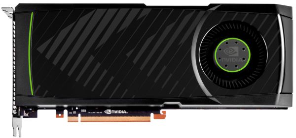
But time heals all wounds. With GF100 out the door NVIDIA has had a chance to examine their design, and TSMC the chance to work the last kinks out of their 40nm process. GF100 was the first Fermi chip, and it would not be the last. With a lesson in hand and a plan in mind, NVIDIA went back to the drawing board to fix and enhance GF100. The end result: GF110, the next iteration of Fermi. Hot out of the oven, it is launching first in the consumer space and is forming the backbone of the first card in NVIDIA’s next GeForce series: GeForce 500. Launching today is the first such card, the GF110-powered GeForce GTX 580.
| GTX 580 | GTX 480 | GTX 460 1GB | GTX 285 | |
| Stream Processors | 512 | 480 | 336 | 240 |
| Texture Address / Filtering | 64/64 | 60/60 | 56/56 | 80 / 80 |
| ROPs | 48 | 48 | 32 | 32 |
| Core Clock | 772MHz | 700MHz | 675MHz | 648MHz |
| Shader Clock | 1544MHz | 1401MHz | 1350MHz | 1476MHz |
| Memory Clock | 1002MHz (4008MHz data rate) GDDR5 | 924MHz (3696MHz data rate) GDDR5 | 900Mhz (3.6GHz data rate) GDDR5 | 1242MHz (2484MHz data rate) GDDR3 |
| Memory Bus Width | 384-bit | 384-bit | 256-bit | 512-bit |
| Frame Buffer | 1.5GB | 1.5GB | 1GB | 1GB |
| FP64 | 1/8 FP32 | 1/8 FP32 | 1/12 FP32 | 1/12 FP32 |
| Transistor Count | 3B | 3B | 1.95B | 1.4B |
| Manufacturing Process | TSMC 40nm | TSMC 40nm | TSMC 40nm | TSMC 55nm |
| Price Point | $499 | ~$420 | ~$190 | N/A |
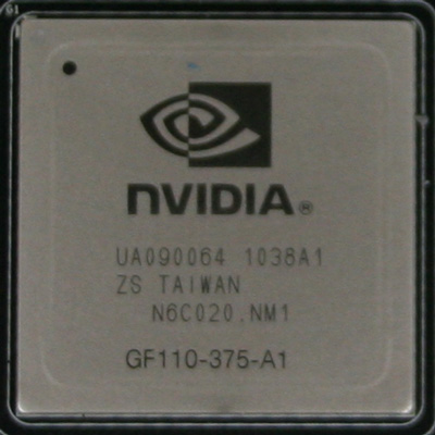
GF110 is a mix of old and new. To call it a brand-new design would be disingenuous, but to call it a fixed GF100 would be equally shortsighted. GF110 does have a lot in common with GF100, but as we’ll see when we get in to the design of GF110 it is its own GPU. In terms of physical attributes it’s very close to GF100; the transistor count remains at 3 billion (with NVIDIA undoubtedly taking advantage of the low precision of that number), while the die size is at 520mm2. NVIDIA never did give us the die size for GF100, but commonly accepted values put it at around 530mm2, meaning GF110 is a hair smaller.
But before we get too deep in to GF110, let’s start with today’s launch card, the GeForce GTX 580. GTX 580 is the first member of the GeForce 500 series, giving it the distinction of setting precedent for the rest of the family that NVIDIA claims will soon follow. Much like AMD last month, NVIDIA is on their second trip with the 40nm process, meaning they’ve had the chance to refine their techniques but not the opportunity to significantly overhaul their designs. As a result the 500 series is going to be very familiar to the 400 series – there really aren’t any surprises or miracle features to talk about. So in many senses, what we’re looking at today is a faster version of the GTX 480.
So what makes GTX 580 faster? We’ll start with the obvious: it’s a complete chip. All the L2 cache, all the ROPs, all the SMs, it’s all enabled. When it comes to gaming this is as fast as GF110 can be, and it’s only through NVIDIA’s artificial FP64 limitations that double-precision computing isn’t equally unrestricted. We have wondered for quite some time what a full GF100 chip would perform like – given that GTX 480 was short on texture units, shaders, and polymorph engines, but not ROPs – and now the answer is at hand. From all of this GTX 580 has 6.6% more shading, texturing, and geometric performance than the GTX 480 at the same clockspeeds. Meanwhile the ROP count and L2 cache remains unchanged; 48 ROPs are attached to 768KB L2 cache, which in turn are attached to 6 64bit memory controllers.
The second change of course is clockspeeds. The reference GTX 480 design ran at 700MHz for the core and 924MHz (3696MHz data rate) for the GDDR5. Meanwhile GTX 580 brings that up to 772MHz for the core and 1002MHz (4008MHz data rate), marking a 72MHz(10%) increase in core clockspeed and a slightly more modest 78MHz (8%) increase in memory bandwidth. This is a near-equal increase in the amount of work that GTX 580 can process and the amount of work its memory can feed it, which should offer a relatively straightforward increase in performance.
Last but certainly not least change coming from GTX 480 is in GF110 itself. NViDIA has ported over GF104’s faster FP16 (half-precision) texture filtering capabilities, giving GF110/GTX580 the ability to filter 4 FP16 pixels per clock, versus 2 on GF100/GTX480. The other change ties in well with the company’s heavy focus on tessellation, with a revised Z-culling/rejection engine that will do a better job of throwing out pixels early, giving GF110/GTX580 more time to spend on rendering the pixels that will actually be seen. This is harder to quantify (and impossible for us to test), but NVIDIA puts this at another 8% performance improvement.
Meanwhile NVIDIA hasn’t ignored GTX 480’s hot and loud history, and has spent some time working on things from that angle. We’ll dive in to NVIDIA’s specific changes later, but the end result is that through some optimization work they’ve managed to reduce their official TDP from 250W on the GTX 480 to 244W on the GTX 580, and in practice the difference is greater than that. NVIDIA’s cooling system of choice has also been updated, working in tandem with GTX 580’s lower power consumption to bring down temperatures and noises. The end result is a card that should be and is cooler and quieter while at the same being faster than GTX 480.
GF110
The downside to this is that if it sounds like a fairy tale, it almost is. As you’ll see we have a rather high opinion of GTX 580, but we’re not convinced you’re going to be able to get one quite yet. NVIDIA is technically hard-launching GTX 580 today at $499 (GTX 480’s old price point), but they aren’t being very talkative about the launch quantity. They claim it’s for competitive reasons (to keep AMD from finding out) and we can certainly respect that, but at the same time it’s rare in this industry for someone to withhold information because it’s a good thing. We really hope to be surprised today and see GTX 580s available for everyone that wants one, but we strongly suspect that it’s going to be available in low quantities and will sell out very quickly. After that it’s anyone’s guess on what the refresh supply will be like; our impression of matters is that yields are reasonable for such a large chip, but that NVIDIA didn’t spend a lot of time stockpiling for today’s launch.
In any case, with GTX 580 taking the $500 spot and GF110 ultimately destined to replace GF100, GF100 based cards are going to be on their way out. NVIDIA doesn’t have an official timeline, but we can’t imagine they’ll continue producing GF100 GPUs any longer than necessary. As a result the GTX 480 and GTX 470 are priced to go, falling between the GTX 580 and the GTX 460 in NVIDIA’s lineup for now until they’re ultimately replaced with other 500 series parts. For the time being this puts the GTX 480 at around $400-$420, and the GTX 470 – still doing battle with the Radeon HD 6870 – is at $239-$259.
Meanwhile AMD does not have a direct competitor for the GTX 580 at the moment, so their closest competition is going to be multi-GPU configurations. In the single card space there’s the Radeon HD 5970, which is destined for replacement soon and as a result AMD is doing what they can to sell off Cypress GPUs by the end of the year. The last reference 5970 you can find on Newegg is a Sapphire card, which is quite blatantly priced against the GTX 580 at $499 with a $30 rebate. Given that it’s the last 5970, we’d be surprised if it was in stock for much longer than the initial GTX 580 shipments.
For cards you do stand a good chance of getting, a pair of 6870s will set you back between $480 and $500, making it a straightforward competitor to the GTX 580 in terms of price. A pair of cards isn’t the best competitor, but CrossFire support is widely available on motherboards so it’s a practical solution at that price.
| Fall 2010 Video Card MSRPs | ||
| NVIDIA | Price | AMD |
|
GeForce GTX 580
|
$500 | Radeon HD 5970 |
| $420 | ||
|
|
$300 | Radeon HD 5870 |
| $240 | Radeon HD 6870 | |
| $180 | Radeon HD 6850 | |
GF110: Fermi Learns Some New Tricks
We’ll start our in-depth look at the GTX 580 with a look at GF110, the new GPU at the heart of the card.
There have been rumors about GF110 for some time now, and while they ultimately weren’t very clear it was obvious NVIDIA would have to follow up GF100 with something else similar to it on 40nm to carry them through the rest of the processes’ lifecycle. So for some time now we’ve been speculating on what we might see with GF100’s follow-up part – an outright bigger chip was unlikely given GF100’s already large die size, but NVIDIA has a number of tricks they can use to optimize things.
Many of those tricks we’ve already seen in GF104, and had you asked us a month ago what we thought GF110 would be, we were expecting some kind of fusion of GF104 and GF100. Primarily our bet was on the 48 CUDA Core SM making its way over to a high-end part, bringing with it GF104’s higher theoretical performance and enhancements such as superscalar execution and additional special function and texture units for each SM. What we got wasn’t quite what we were imagining – GF110 is much more heavily rooted in GF100 than GF104, but that doesn’t mean NVIDIA hasn’t learned a trick or two.
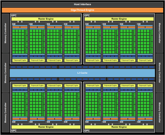
Fundamentally GF110 is the same architecture as GF100, especially when it comes to compute. 512 CUDA Cores are divided up among 4 GPCs, and in turn each GPC contains 1 raster engine and 4 SMs. At the SM level each SM contains 32 CUDA cores, 16 load/store units, 4 special function units, 4 texture units, 2 warp schedulers with 1 dispatch unit each, 1 Polymorph unit (containing NVIDIA’s tessellator) and then the 48KB+16KB L1 cache, registers, and other glue that brought an SM together. At this level NVIDIA relies on TLP to keep a GF110 SM occupied with work. Attached to this are the ROPs and L2 cache, with 768KB of L2 cache serving as the guardian between the SMs and the 6 64bit memory controllers. Ultimately GF110’s compute performance per clock remains unchanged from GF100 – at least if we had a GF100 part with all of its SMs enabled.
On the graphics side however, NVIDIA has been hard at work. They did not port over GF104’s shader design, but they did port over GF104’s texture hardware. Previously with GF100, each unit could compute 1 texture address and fetch 4 32bit/INT8 texture samples per clock, 2 64bit/FP16 texture samples per clock, or 1 128bit/FP32 texture sample per clock. GF104’s texture units improved this to 4 samples/clock for 32bit and 64bit, and it’s these texture units that have been brought over for GF110. GF110 can now do 64bit/FP16 filtering at full speed versus half-speed on GF100, and this is the first of the two major steps NVIDIA took to increase GF110’s performance over GF100’s performance on a clock-for-clock basis.
| NVIDIA Texture Filtering Speed (Per Texture Unit) | |||||
| GF110 | GF104 | GF100 | |||
| 32bit (INT8) | 4 Texels/Clock | 4 Texels/Clock | 4 Texels/Clock | ||
| 64bit (FP16) | 4 Texels/Clock | 4 Texels/Clock | 2 Texels/Clock | ||
| 128bit (FP32) | 1 Texel/Clock | 1 Texel/Clock | 1 Texel/Clock | ||
Like most optimizations, the impact of this one is going to be felt more on newer games than older games. Games that make heavy use of 64bit/FP16 texturing stand to gain the most, while older games that rarely (if at all) used 64bit texturing will gain the least. Also note that while 64bit/FP16 texturing has been sped up, 64bit/FP16 rendering has not – the ROPs still need 2 cycles to digest 64bit/FP16 pixels, and 4 cycles to digest 128bit/FP32 pixels.
It’s also worth noting that this means that NVIDIA’s texture:compute ratio schism remains. Compared to GF100, GF104 doubled up on texture units while only increasing the shader count by 50%; the final result was that per SM 32 texels were processed to 96 instructions computed (seeing as how the shader clock is 2x the base clock), giving us 1:3 ratio. GF100 and GF110 on the other hand retain the 1:4 (16:64) ratio. Ultimately at equal clocks GF104 and GF110 widely differ in shading, but with 64 texture units total in both designs, both have equal texturing performance.
Moving on, GF110’s second trick is brand-new to GF110, and it goes hand-in-hand with NVIDIA’s focus on tessellation: improved Z-culling. As a quick refresher, Z-culling is a method of improving GPU performance by throwing out pixels that will never be seen early in the rendering process. By comparing the depth and transparency of a new pixel to existing pixels in the Z-buffer, it’s possible to determine whether that pixel will be seen or not; pixels that fall behind other opaque objects are discarded rather than rendered any further, saving on compute and memory resources. GPUs have had this feature for ages, and after a spurt of development early last decade under branded names such as HyperZ (AMD) and Lightspeed Memory Architecture (NVIDIA), Z-culling hasn’t been promoted in great detail since then.

Z-Culling In Action: Not Rendering What You Can't See
For GF110 this is changing somewhat as Z-culling is once again being brought back to the surface, although not with the zeal of past efforts. NVIDIA has improved the efficiency of the Z-cull units in their raster engine, allowing them to retire additional pixels that were not caught in the previous iteration of their Z-cull unit. Without getting too deep into details, internal rasterizing and Z-culling take place in groups of pixels called tiles; we don’t believe NVIDIA has reduced the size of their tiles (which Beyond3D estimates at 4x2); instead we believe NVIDIA has done something to better reject individual pixels within a tile. NVIDIA hasn’t come forth with too many details beyond the fact that their new Z-cull unit supports “finer resolution occluder tracking”, so this will have to remain a mystery for another day.
In any case, the importance of this improvement is that it’s particularly weighted towards small triangles, which are fairly rare in traditional rendering setups but can be extremely common with heavily tessellated images. Or in other words, improving their Z-cull unit primarily serves to improve their tessellation performance by allowing NVIDIA to better reject pixels on small triangles. This should offer some benefit even in games with fewer, larger triangles, but as framed by NVIDIA the benefit is likely less pronounced.
In the end these are probably the most aggressive changes NVIDIA could make in such a short period of time. Considering the GF110 project really only kicked off in earnest in February, NVIDIA only had around half a year to tinker with the design before it had to be taped out. As GPUs get larger and more complex, the amount of tweaking that can get done inside such a short window is going to continue to shrink – and this is a far cry from the days where we used to get major GPU refreshes inside of a year.
Keeping It Cool: Transistors, Throttles, and Coolers
Beyond the specific architectural improvements for GF110 we previously discussed, NVIDIA has also been tinkering with their designs at a lower level to see what they could do to improve their performance in conjunction with TSMC’s 40nm manufacturing process. GF100/GTX480 quickly gathered a reputation as a hot product, and this wasn’t an unearned reputation. Even with an SM fused off, GTX 480 already had a TDP of 250W, and the actual power draw could surpass that in extreme load situations such as FurMark.
NVIDIA can (and did) tackle things on the cooling side of things by better dissipating that heat, but keeping their GPUs from generating it in the first place was equally important. This was especially important if they wanted to push high-clocked fully-enabled designs on to the consumer GeForce and HPC Tesla markets, with the latter in particular not being a market where you can simply throw more cooling at the problem. As a result NVIDIA had to look at GF110 at a transistor level, and determine what they could do to cut power consumption.
Semiconductors are a near-perfect power-to-heat conversion device, so a lot of work goes in to getting as much work done with as little power as necessary. This is compounded by the fact that dynamic power (which does useful work) only represents some of the power used – the rest of the power is wasted as leakage power. In the case of a high-end GPU NVIDIA doesn’t necessarily want to reduce dynamic power usage and have it impact performance, instead they want to go after leakage power. This in turn is compounded by the fact that leaky transistors and high clocks are strange bedfellows, making it difficult to separate the two. The result is that leaky transistors are high-clocking transistors, and vice versa.
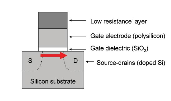
A typical CMOS transitor: Thin gate dielectrics lead to leakage
Thus the trick to making a good GPU is to use leaky transistors where you must, and use slower transistors elsewhere. This is exactly what NVIDIA did for GF100, where they primarily used 2 types of transistors differentiated in this manner. At a functional unit level we’re not sure which units used what, but it’s a good bet that most devices operating on the shader clock used the leakier transistors, while devices attached to the base clock could use the slower transistors. Of course GF100 ended up being power hungry – and by extension we assume leaky anyhow – so that design didn’t necessarily work out well for NVIDIA.
For GF110, NVIDIA included a 3rd type of transistor, which they describe as having “properties between the two previous ones”. Or in other words, NVIDIA began using a transistor that was leakier than a slow transistor, but not as leaky as the leakiest transistors in GF100. Again we don’t know which types of transistors were used where, but in using all 3 types NVIDIA ultimately was able to lower power consumption without needing to slow any parts of the chip down. In fact this is where virtually all of NVIDIA’s power savings come from, as NVIDIA only outright removed few if any transistors considering that GF110 retains all of GF100’s functionality.
Of course reducing leakage is one way to reduce power consumption, but it doesn’t solve NVIDIA’s other problems in hitting their desired TDP. Both NVIDIA and AMD base their GPU TDP specifications around “real world” applications and games, with NVIDIA largely viewed to be more aggressive on this front. In either case load-generating programs like FurMark and OCCT do not exist in AMD or NVIDIA’s worlds, leading both companies to greatly despise these programs and label them as “power viruses” and other terms.
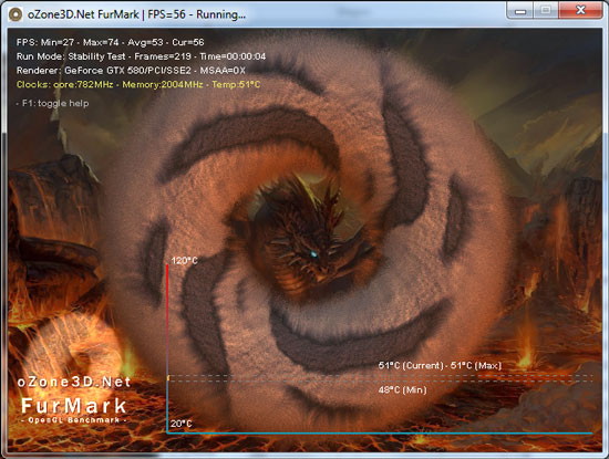
After a particularly rocky relationship with FurMark blowing up VRMs on the Radeon 4000 series, AMD instituted safeties in their cards with the 5000 series to protect against FurMark – AMD monitored the temperature of the VRMs, and would immediately downclock the GPU if the VRM temperatures exceeded specifications. Ultimately as this was temperature based AMD’s cards were allowed to run to the best of their capabilities, so long as they weren’t going to damage themselves. In practice we rarely encountered AMD’s VRM protection even with FurMark except in overclocking scenarios, where overvolting cards such as the 5970 quickly drove up the temperature of the VRMs.
For GTX 580 NVIDIA is taking an even more stringent approach than AMD, as they’ll be going after power consumption itself rather than just focusing on protecting the card. Attached to GTX 580 are a series of power monitoring chips, which monitor the amount of power the card is drawing from the PCIe slot and PCIe power plugs. By collecting this information NVIDIA’s drivers can determine if the card is drawing too much power, and slow the card down to keep it within spec. This kind of power throttling is new for GPUs, though it’s been common with CPUs for a long time.
NVIDIA’s reasoning for this change doesn’t pull any punches: it’s to combat OCCT and FurMark. At an end-user level FurMark and OCCT really can be dangerous – even if they can’t break the card any longer, they can still cause other side-effects by drawing too much power from the PSU. As a result having this protection in place more or less makes it impossible to toast a video card or any other parts of a computer with these programs. Meanwhile at a PR level, we believe that NVIDIA is tired of seeing hardware review sites publish numbers showcasing GeForce products drawing exorbitant amounts of power even though these numbers represent non-real-world scenarios. By throttling FurMark and OCCT like this, we shouldn’t be able to get their cards to pull so much power. We still believe that tools like FurMark and OCCT are excellent load-testing tools for finding a worst-case scenario and helping our readers plan system builds with those scenarios in mind, but at the end of the day we can’t argue that this isn’t a logical position for NVIDIA.
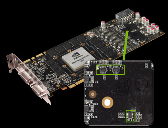
Power Monitoring Chips Identified
While this is a hardware measure the real trigger is in software. FurMark and OCCT are indeed throttled, but we’ve been able to throw other programs at the GTX 580 that cause a similar power draw. If NVIDIA was actually doing this all in hardware everything would be caught, but clearly it’s not. For the time being this simplifies everything – you need not worry about throttling in anything else whatsoever – but there will be ramifications if NVIDIA actually uses the hardware to its full potential.
Much like GDDR5 EDC complicated memory overclocking, power throttling would complicate overall video card overclocking, particularly since there’s currently no way to tell when throttling kicks in. On AMD cards the clock drop is immediate, but on NVIDIA’s cards the drivers continue to report the card operating at full voltage and clocks. We suspect NVIDIA is using a NOP or HLT-like instruction here to keep the card from doing real work, but the result is that it’s completely invisible even to enthusiasts. At the moment it’s only possible to tell if it’s kicking in if an application’s performance is too low. It goes without saying that we’d like to have some way to tell if throttling is kicking in if NVIDIA fully utilizes this hardware.
Finally, with average and maximum power consumption dealt with, NVIDIA turned to improving cooling on the GTX to bring temperatures down and to more quietly dissipate heat. GTX 480 not only was loud, but it had an unusual cooling design that while we’re fine with, ended up raising eyebrows elsewhere. Specifically NVIDIA had heatpipes sticking out of the GTX 480, an exposed metal grill over the heatsink, and holes in the PCB on the back side of the blower to allow it to breathe from both sides. Considering we were dissipating over 300W at times it was effective, but apparently not a design NVIDIA liked.
So for GTX 580 NVIDIA has done a lot of work under the hood to produce a card that looks less like the GTX 480 and more like the all-enclosed coolers we saw with the GTX 200 series; the grill, external heatpipes, and PCB ventilation holes are all gone from the GTX 580, and no one would hold it against you to mistake it for a GTX 285. The biggest change in making this possible is NVIDIA’s choice of heatsink: NVIDIA has ditched traditional heatpipes and gone to the new workhorse of vapor chamber cooling.
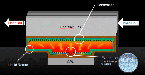
A Vapor Chamber Cooler In Action (Courtesy NVIDIA)
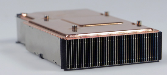
The GTX 580's Vapor Chamber + Heatsink
Vapor chamber coolers have been around for quite some time as aftermarket/custom coolers, and are often the signature design element for Sapphire; it was only more recently with the Radeon HD 5970 that we saw one become part of a reference GPU design. NVIDIA has gone down the same road and is now using a vapor chamber for the reference GTX 580 cooler. Visually this means the heatpipes are gone, while internally this should provide equal if not better heat conduction between the GPU’s heatspreader and the aluminum heatsink proper. The ultimate benefit from this being that with better heat transfer it’s not necessary to run the blower so hard to keep the heatsink cooler in order to maximize the temperature difference between the heatsink and GPU.
NVIDIA’s second change was to the blower itself, which is the source of all noise. NVIDIA found that the blower on the GTX 480 was vibrating against itself, producing additional noise and in particular the kind of high-pitch whining that makes a cooler come off as noisy. As a result NVIDIA has switched out the blower for a slightly different design that keeps a ring of plastic around the top, providing more stability. This isn’t a new design – it’s on all of our Radeon HD 5800 series cards – but much like the vapor chamber this is the first time we’ve seen it on an NVIDIA reference card.
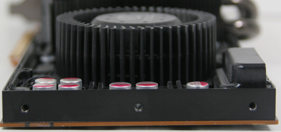
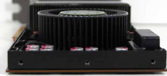
Top: GTX 480 Blower. Bottom: GTX 580 Blower
Finally, NVIDIA has also tinkered with the shape of the shroud encasing the card for better airflow. NVIDIA already uses a slightly recessed shroud near the blower in order to allow some extra space between it and the next card, but they haven’t done anything with the overall shape until now. Starting with the GTX 580, the shroud is now slightly wedge-shaped between the blower and the back of the card; this according to NVIDIA improves airflow in SLI setups where there’s a case fan immediately behind the card by funneling more fresh air in to the gap between cards.
Meet the GTX 580
Since we’ve already discussed the cooling, let’s dive right in to the rest of the GTX 580, shall we?
Launching today will be a single GTX 580 design, the reference design. Talking to our contacts, semi-custom designs (designs using the reference PCB with a different cooler) are due in the next few weeks assuming everything goes to plan and of course there’s ample supply. And while we’re on that note, NVIDIA let us know that with their focus on cooling on the GTX 580 they aren’t going to be letting custom GTX 580 designs go out without a more thorough inspection. The acoustic performance of the reference GTX 580 is going to be the bare minimum to get a design approved – if it can’t beat the reference design, NVIDIA won’t allow it. We consider this a matter of brand protection for the company, as a bad/loud GeForce is still a GeForce all the same.
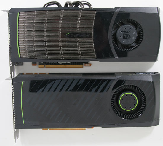
Top: GTX 480. Bottom: GTX580
With the reference design the resulting card is very close to being a GTX 285/480 hybrid. In terms of overall design it ends up looking very similar to the GTX 285. At 10.5” long it’s the same length as the GTX 480 or a smidge longer than the GTX 285, and should fit in to any cases those cards could work in. Power connectivity is the same as the GTX 480, with 6pin and 8pin PCIe sockets being located at the top of the card, providing easy access to the sockets. At 244W TDP the card draws too much for 6+6, but you can count on an eventual GTX 570 to fill that niche. Meanwhile NVIDIA has kept the 480’s detachable shroud lid, meaning you can remove the cover of the shroud without disturbing the rest of the card; it’s worth noting that it’s secured with screws rather than laches this time however.
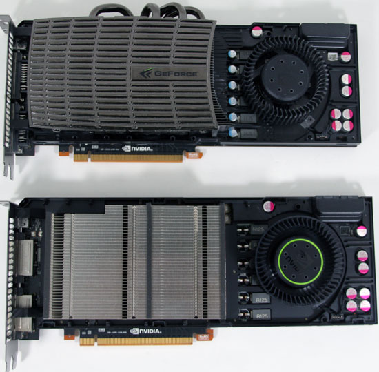
Heatsinks Exposed! Top: GTX 480. Bottom: GTX 580
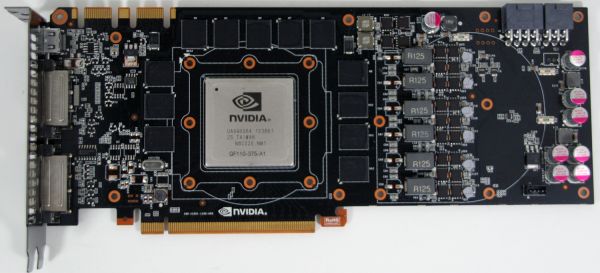
On the front side of the PCB you’ll find the 12 GDDR5 chips composing the card’s 384bit memory bus. The thermal pads connecting the memory to the shroud have once again wiped out the chip markings, so we haven’t been able to determine what these chips are, although we’re confident they’re 5Gbps like in past cards. At the center of the card is the GF110 GPU encased in a metal heatspreader, a common sight for NVIDIA’s high-end GPUs. This is an A1 revision GPU, which in NVIDIA’s counting system means it’s the first tape-out. Elsewhere on the board you’ll find the 2 SLI connectors, providing support for tri-SLI on the 580. All told while the GPU has been refined, the PCB remains largely unchanged from the GTX 480 other than removing the ventilation holes – all of the ICs are in practically the same place, and even the VRM controller is the same.
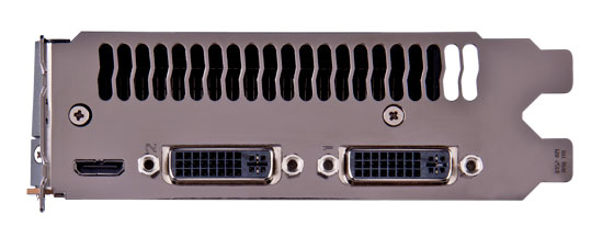
Meanwhile looking at the IO bracket for the 580, we find the same configuration as we saw on the 480. Below a full-sized vent are 2 DVI ports and a mini-HDMI port. NVIDIA slightly revised their display controller for GF110/GTX580; the good news is that HDMI 1.4a is supported, the bad news is that full audio bitstreaming is not supported so it’s the same as it was on the GTX 480: 8 channel LPCM and lossy audio formats like DD+ and DTS. This actually caught us off-guard since we were expecting the full GF104 treatment here, but it just goes to show that this is a GF100-derrivative after all. Unfortunately this also extends to the number of displays supported – NVIDIA still only supports 2 displays on one card, so you need to run in SLI if you intend to take advantage of 3DVision/NVIDIA surround across 3 monitors.
Finally, it’s with some sense of irony that we find ourselves yelling more at AMD than NVIDIA for naming shenanigans this time around, considering it was NVIDIA that brought us the 8800GT/9800GT and GeForce 200/300 product naming snafus. While NVIDIA has made some changes compared to the GTX 480, it’s a very short list; shorter than even AMD’s list for the 6800 series. At the same time, at least the GTX 580 is faster than the GTX 480 versus AMD’s 6800/5800 series. Quite frankly the GTX 580 should be the GTX 485 – the few architectural changes we’ve seen do make a difference, but then NVIDIA did a whole die shrink on the GTX 280 and only got a GTX 285 out of it. Both companies seem committed to coming out with a new family of video cards this year regardless of where the GPU powering them has actually changed. Ultimately the GTX 580 is the second flimsiest excuse for a new series number, next only to simply rebranding an existing GPU.
The Test
For our look at the GTX 580 we will only be looking at single card performance. As a measure of promotion for their OEM partners, NVIDIA would only make a second GTX 580 available to us if we also agreed to review a high-end gaming system. Because the high-end system was completely unnecessary for a GPU review we declined NVIDIA’s offer, and as a result we were only offered 1 GTX 580 which you’ll be seeing here today. We will be looking at SLI performance once we can acquire a second GTX 580 farther down the line.
For our testing we’ll be using the latest version of our GPU benchmark suite, which was introduced back in our Radeon HD 6800 series review two weeks ago. We’re using the latest drivers from both AMD and NVIDIA here – Catalyst Hotfix 10.10d for AMD, and Forceware 262.99 for the NVIDIA cards.
Finally, as we mentioned earlier, AMD doesn’t have a direct competitor to the GTX 580. The closest competitors they have are dual-GPU setups in the form of the closeout 5970 and the 6870 in Crossfire. Meanwhile NVIDIA has cut GTX 470 prices so far to the bone that you can pick up a pair of them for as much as a single GTX 580. Two slightly crippled GF100 cards versus one GF110 card will not be a fair fight…
| CPU: | Intel Core i7-920 @ 3.33GHz |
| Motherboard: | Asus Rampage II Extreme |
| Chipset Drivers: | Intel 9.1.1.1015 (Intel) |
| Hard Disk: | OCZ Summit (120GB) |
| Memory: | Patriot Viper DDR3-1333 3 x 2GB (7-7-7-20) |
| Video Cards: |
AMD Radeon HD 6870 AMD Radeon HD 6850 AMD Radeon HD 5970 AMD Radeon HD 5870 AMD Radeon HD 5850 AMD Radeon HD 5770 AMD Radeon HD 4870 NVIDIA GeForce GTX 580 NVIDIA GeForce GTX 480 NVIDIA GeForce GTX 470 NVIDIA GeForce GTX 460 1GB NVIDIA GeForce GTX 460 768MB NVIDIA GeForce GTX 285 NVIDIA GeForce GTX 260 Core 216 |
| Video Drivers: |
NVIDIA ForceWare 262.99 AMD Catalyst 10.10d |
| OS: | Windows 7 Ultimate 64-bit |
Crysis: Warhead
Kicking things off as always is Crysis: Warhead, still one of the toughest game in our benchmark suite. Even 2 years since the release of the original Crysis, “but can it run Crysis?” is still an important question, and the answer continues to be “no.” One of these years we’ll actually be able to run it with full Enthusiast settings…
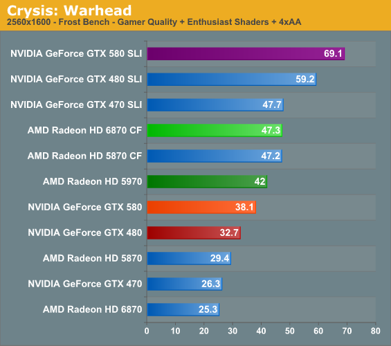
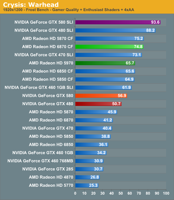
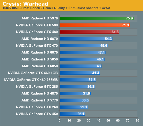
Right off the bat we see the GTX 580 do well, which as the successor to what was already the fastest single-GPU card on the market is nothing less than we expect. At 2560 it’s around 16% faster than the GTX 480, and at 1920 that drops to 12%. Bear in mind that the theoretical performance improvement for clock + shader is 17%, so in reality it would be nearly impossible get that close without the architectural improvements also playing a role.
Meanwhile AMD’s double-GPU double-trouble lineup of the 5970 and 6870CF both outscore the GTX 580 by around 12% and 27% respectively. It shouldn’t come as a shock that they’re going to win most tests – ultimately they’re priced much more competitively than the GTX 580, making them price-practical alternatives to the GTX 580.
And speaking of competition the GTX 470 SLI is in much the same boat, handily surpassing the GTX 580. This will come full circle however when we look at power consumption.
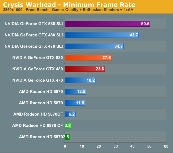
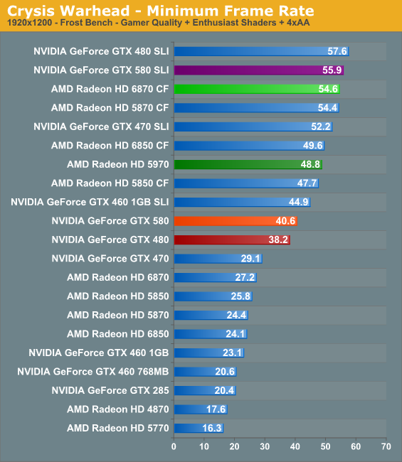
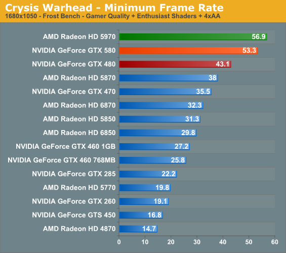
Meanwhile looking at minimum framerates we have a different story. AMD’s memory management in CrossFire mode has long been an issue with Crysis at 2560, and it continues to show here with a minimum framerate that simply craters. At 2560 there’s a world of difference between NVIDIA and AMD here, and it’s all in NVIDIA’s favor. 1920 however roughly mirrors our earlier averages, with the 580 taking a decent lead over the GTX 480, but falling to multi-GPU cards.
BattleForge DX10
Up next is BattleForge, Electronic Arts’ free to play online RTS. As far as RTSes go this game can be quite demanding, and this is without the game’s DX11 features.
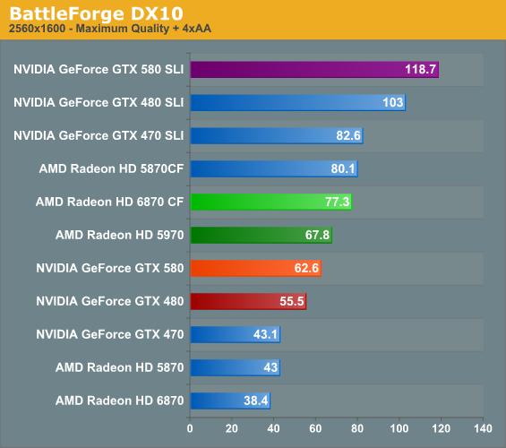
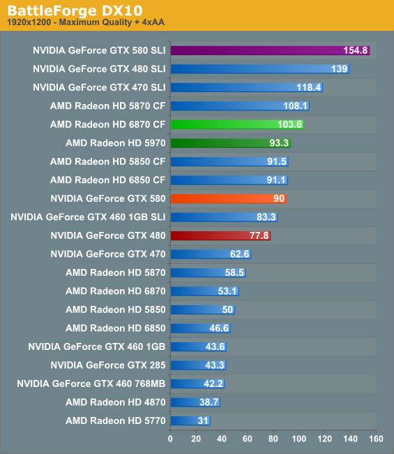
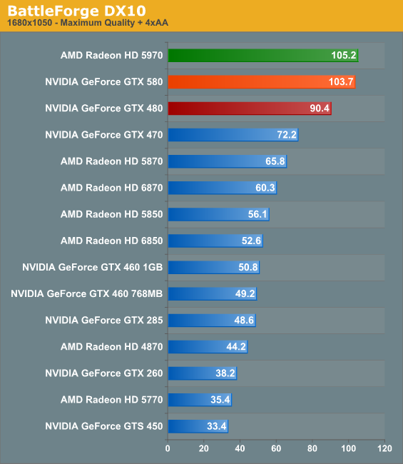
BattleForge is one of the better examples of an “average” game for the GTX 580 compared to the GTX 480. At around 14% faster, it’s not too far off from the global average. Meanwhile the SLI and Crossfire setups pull ahead, but this time the GTX 580 is much closer to the 5970 and 6870CF.
Metro 2033
The first recently added game on our list is 4A Games’ Metro 2033, their tunnel shooter released earlier this year. In September the game finally received a major patch resolving some outstanding image quality issues with the game, finally making it suitable for use in our benchmark suite. At the same time a dedicated benchmark mode was added to the game, giving us the ability to reliably benchmark much more stressful situations than we could with FRAPS. If Crysis is a tropical GPU killer, then Metro would be its underground counterpart.
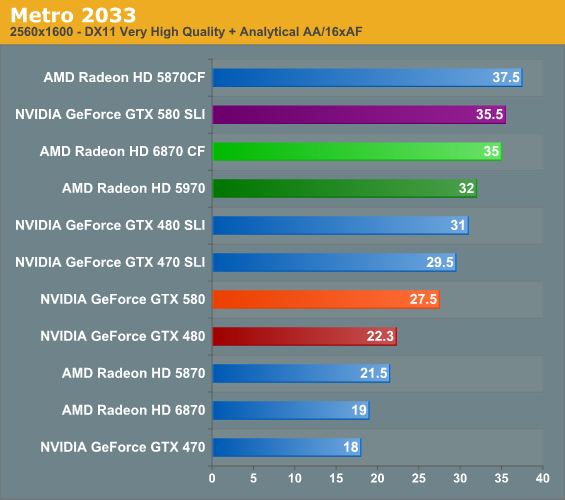
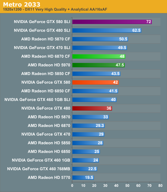
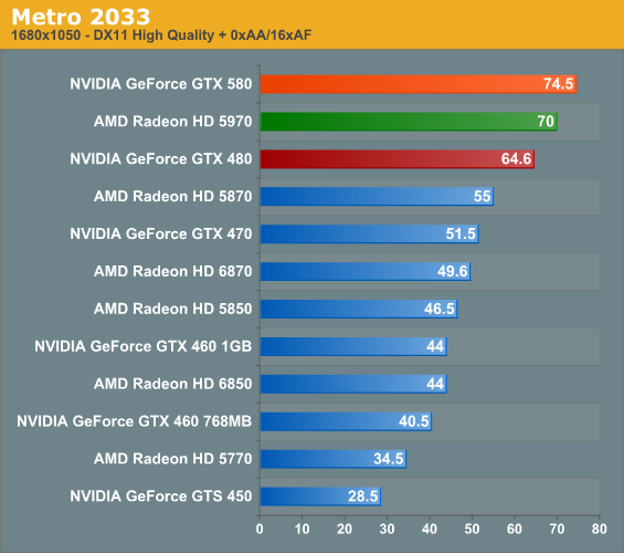
If BattleForge is an average game for the GTX 580, then Metro would be an outstanding game. Compared to the GTX 480 it’s 23% faster at 2560, falling off at lower resolutions. While the difference isn't earthshattering, it’s big enough that even at 1920 it’s just enough to push the framerate in to a more comfortable range. CrossFire/SLI push the envelope further, bringing the framerate up to playable levels at 2560, and increasing the spread at 1920. And finally at 1680 with lower settings we can finally crack 60fps with 1 card, but it’s going to take a GTX 480, 580, or 5970 to do it.
HAWX
Ubisoft’s 2008 aerial action game is one of the less demanding games in our benchmark suite, particularly for the latest generation of cards. However it’s fairly unique in that it’s one of the few flying games of any kind that comes with a proper benchmark.
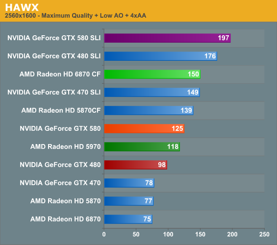
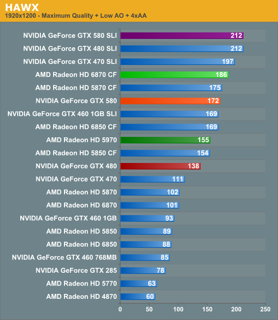
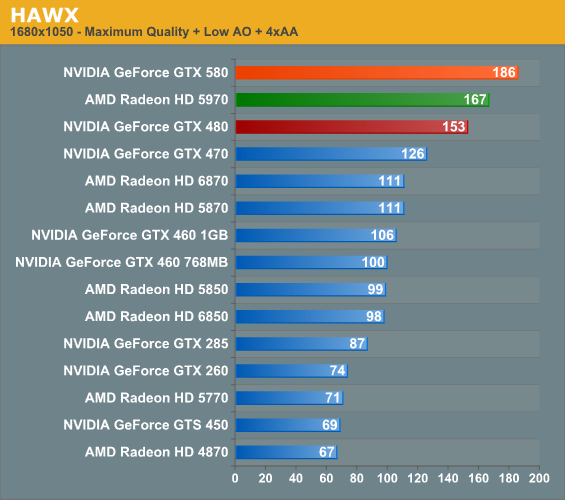
Throughout all of our testing it’s HAWX that ends up being the best game for the GTX 580 compared to its predecessor. At 2560 the difference is a staggering 27%, and even at 1920 it’s still 25%. HAWX as far as we know is not huge on FP16 texture filtering, so it may be the biggest benefactor of the Z-culling improvements for GF110.
It actually does well enough here that this is one of the few times even the 5970 can’t keep up; the difference is under 10%, but we wouldn’t normally expect the 580 to surpass AMD’s double-GPU monster.
Civilization V
The other new game in our benchmark suite is Civilization 5, the latest incarnation in Firaxis Games’ series of turn-based strategy games. Civ 5 gives us an interesting look at things that not even RTSes can match, with a much weaker focus on shading in the game world, and a much greater focus on creating the geometry needed to bring such a world to life. In doing so it uses a slew of DirectX 11 technologies, including tessellation for said geometry and compute shaders for on-the-fly texture decompression.
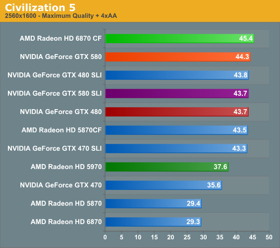
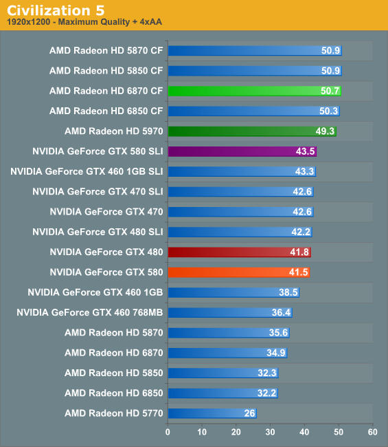
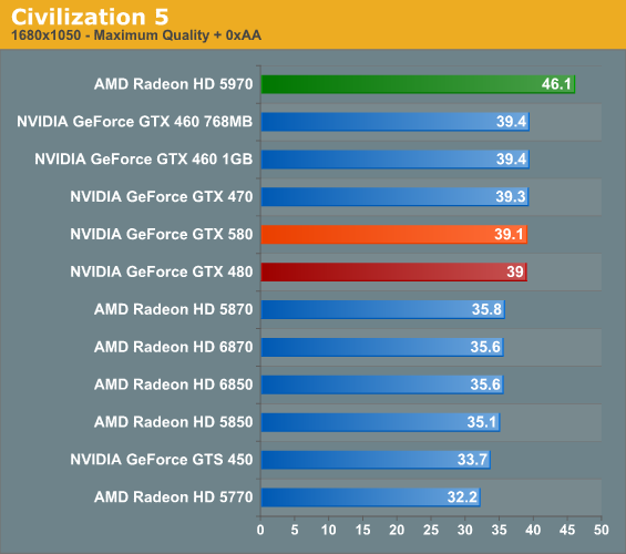
Civilization V continues to vex us for a couple different reasons. For all the DirectX 11 bells and whistles it uses, it’s definitely CPU limited at times. And on the other hand, adding a second GPU definitely helps, but only for AMD, as NVIDIA even with a Civilization V SLI profile is gaining practically nothing. Finally, those GTX 480 and 580 numbers aren’t wrong – it really does get faster at higher resolutions for reasons we can only assume are due to the triangles getting larger and easier to rasterize and/or cull.
In any case the GTX 580 still manages to nearly top the charts at 2560, as in lieu of good SLI/CF scaling, the biggest single GPU is worth having. Ultimately we appear to be CPU limited at this resolution, which for reasons unknown doesn’t bode well for the 5970. Meanwhile at 1920 the picture gets turned on its head, with the GTX 580 effectively tying the GTX 480 here while at the same time AMD’s mutli-GPU configurations pull ahead.
Battlefield: Bad Company 2
The latest game in the Battlefield series - Bad Company 2 – remains as one of the cornerstone DX11 games in our benchmark suite. As BC2 doesn’t have a built-in benchmark or recording mode, here we take a FRAPS run of the jeep chase in the first act, which as an on-rails portion of the game provides very consistent results and a spectacle of explosions, trees, and more.
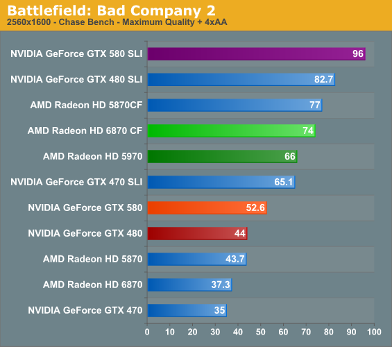
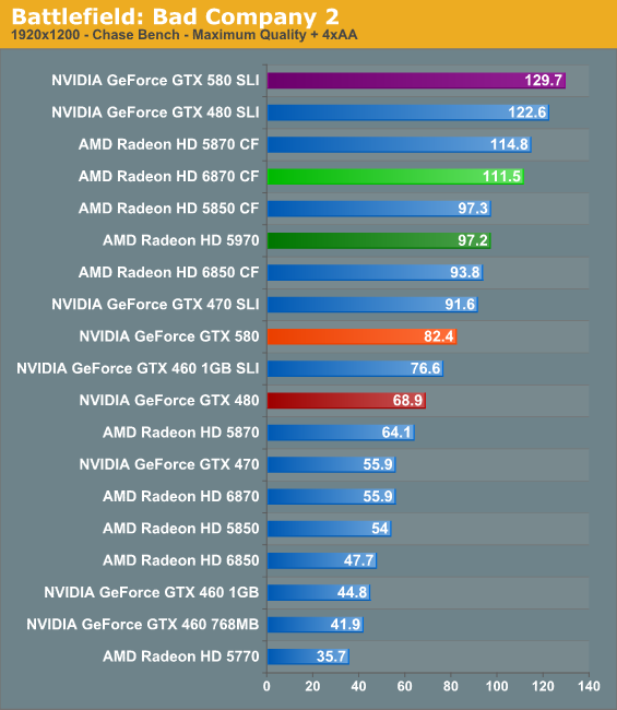
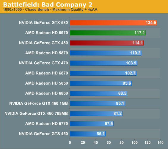
Compared to the GTX 480, the GTX 580 has a rather straightforward 20% lead at both 2560 and 1920, once again surpassing our theoretical shader + clock numbers. Meanwhile in the SLI/CF camp this game has always favored AMD, so it’s not surprising to see the GTX 580 fall well behind the AMD multi-GPU solutions.
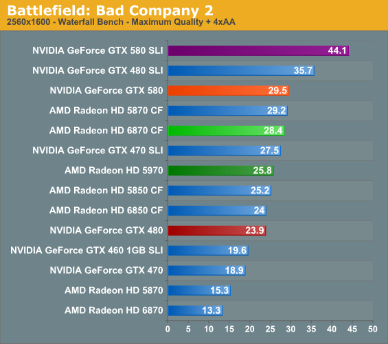
The waterfall minimum framerate test on the other hand usually erases any AMD lead and this is no exception. In spite of the GTX 580’s notably lower average framerate, here it pops ahead of its peers and falls just short of 30fps. Given the MP-centric design of the game, this could very well be the more important chart to look at.
STALKER: Call of Pripyat
The third game in the STALKER series continues to build on GSC Game World’s X-Ray Engine by adding DX11 support, tessellation, and more. This also makes it another one of the highly demanding games in our benchmark suite.
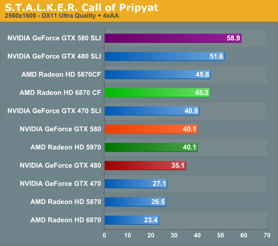
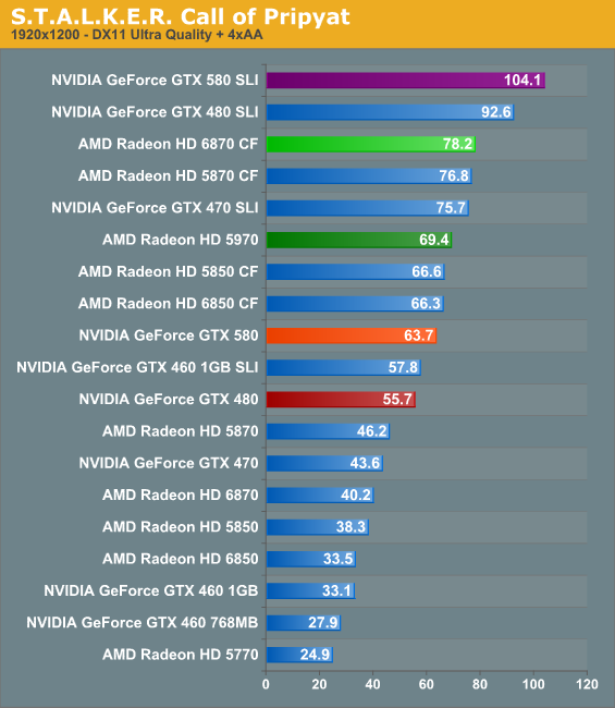
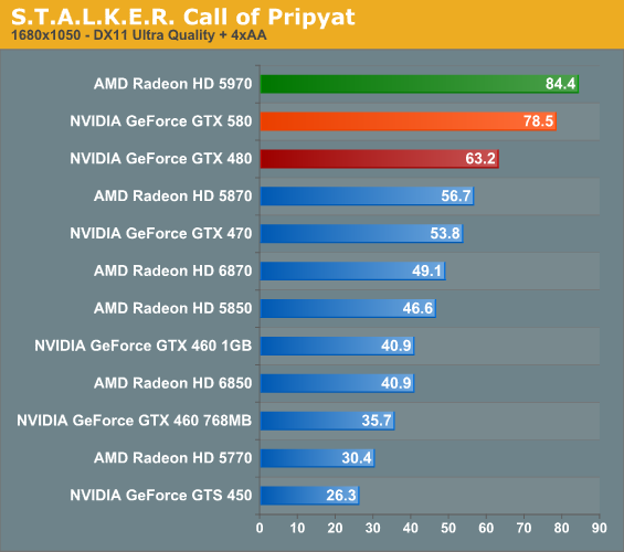
STALKER ends up being a mixed bag for NVIDIA, depending on the competition. The GTX 580 still holds a solid lead over the GTX 480, but it’s not as great as in other games. Meanwhile the GTX 580 can tie the 5970 at 2560 before falling behind at 1920. It’s worth noting that among single-GPU cards, the 580 does become the first and only card to crack 60fps at 1920.
DIRT 2
Codemasters’ 2009 off-road racing game continues its reign as the token racer in our benchmark suite. As the first DX11 racer, DIRT 2 makes pretty thorough use of the DX11’s tessellation abilities, not to mention still being the best looking racer we have ever seen.
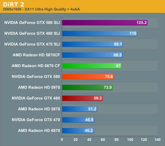
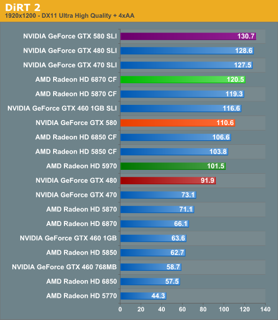
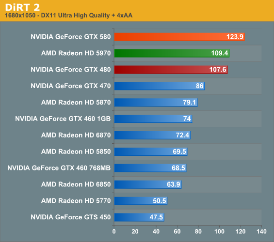
NVIDIA has in the past and continues to do rather well in DIRT 2, an amusing outcome given that this was an AMD promoted game. The GTX 580 is not only over 20% faster over the GTX 480, but enjoys a small lead over even the 5970, falling to only the 6870 CF. Not that it’s hard to do well here; even the GTX 480 can almost hit 60fps at 2560.
Mass Effect 2
Electronic Arts’ space-faring RPG is our Unreal Engine 3 game. While it doesn’t have a built in benchmark, it does let us force anti-aliasing through driver control panels, giving us a better idea of UE3’s performance at higher quality settings. Since we can’t use a recording/benchmark in ME2, we use FRAPS to record a short run.
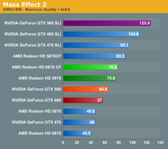
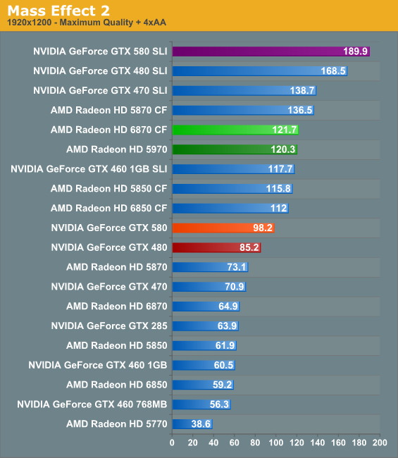
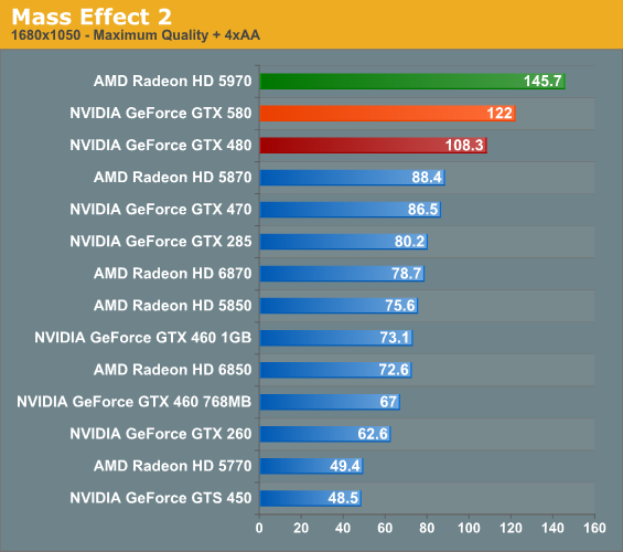
Mass Effect 2 has always surprised us by just how strenuous it is, even though UE3 is intended to be flexible to reach a wide range of systems. Furthermore it doesn’t seem to benefit nearly as much from the GTX 580 as other games, with the performance advantage over the GTX 480 shrinking to around 13%. The ultimate victor ends up being the AMD multi-GPU setups, and farther above that still is the GTX 470 SLI.
Wolfenstein
Finally among our revised benchmark suite we have Wolfenstein, the most recent game to be released using the id Software Tech 4 engine. All things considered it’s not a very graphically intensive game, but at this point it’s the most recent OpenGL title available. It’s more than likely the entire OpenGL landscape will be thrown upside-down once id releases Rage next year.
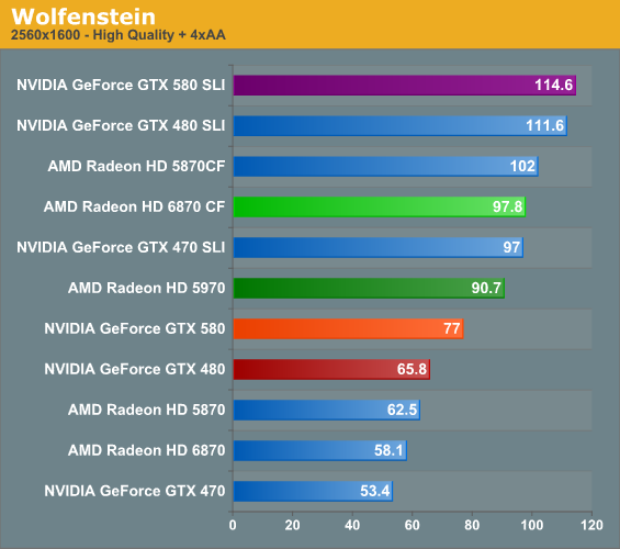
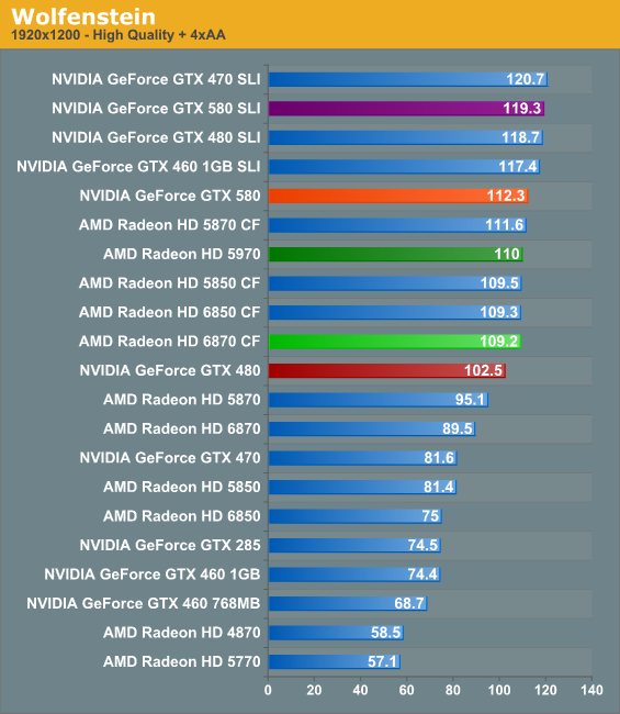
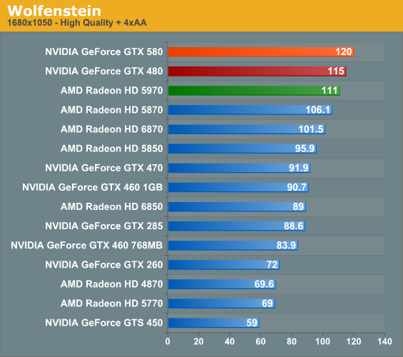
Wolfenstein ends up getting CPU bound rather quickly, particularly with multi-GPU in the mix. Only at 2560 can these cards really get out and stretch their legs, and even the 480 SLI is likely approaching the cap. With that in mind the GTX 580 ends up splitting the difference between the GTX 480 and 5970 – the 5970 is around 17% faster than the 580, followed by the 580 being about the same difference from the 480.
Compute and Tessellation
Moving on from our look at gaming performance, we have our customary look at compute performance, bundled with a look at theoretical tessellation performance. Unlike our gaming benchmarks where NVIDIA’s architectural enhancements could have an impact, everything here should be dictated by the core clock and SMs, with shader and polymorph engine counts defining most of these tests.
Our first compute benchmark comes from Civilization V, which uses DirectCompute to decompress textures on the fly. Civ V includes a sub-benchmark that exclusively tests the speed of their texture decompression algorithm by repeatedly decompressing the textures required for one of the game’s leader scenes.
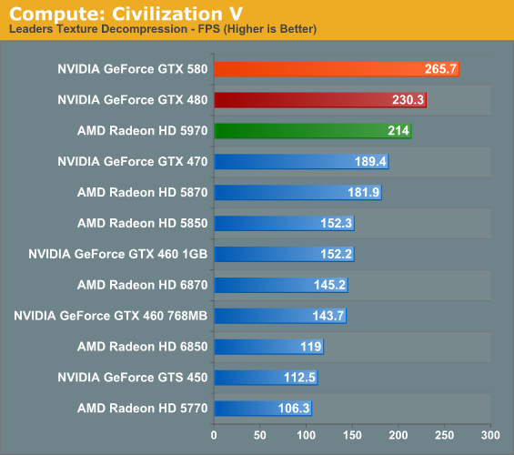
We previously discovered that NVIDIA did rather well in this test, so it shouldn’t come as a surprise that the GTX 580 does even better. Even without the benefits of architectural improvements, the GTX 580 still ends up pulling ahead of the GTX 480 by 15%. The GTX 580 also does well against the 5970 here, which does see a boost from CrossFire but ultimately falls short, showcasing why multi-GPU cards can be inconsistent at times.
Our second compute benchmark is Cyberlink’s MediaEspresso 6, the latest version of their GPU-accelerated video encoding suite. MediaEspresso 6 doesn’t currently utilize a common API, and instead has codepaths for both AMD’s APP (née Stream) and NVIDIA’s CUDA APIs, which gives us a chance to test each API with a common program bridging them. As we’ll see this doesn’t necessarily mean that MediaEspresso behaves similarly on both AMD and NVIDIA GPUs, but for MediaEspresso users it is what it is.
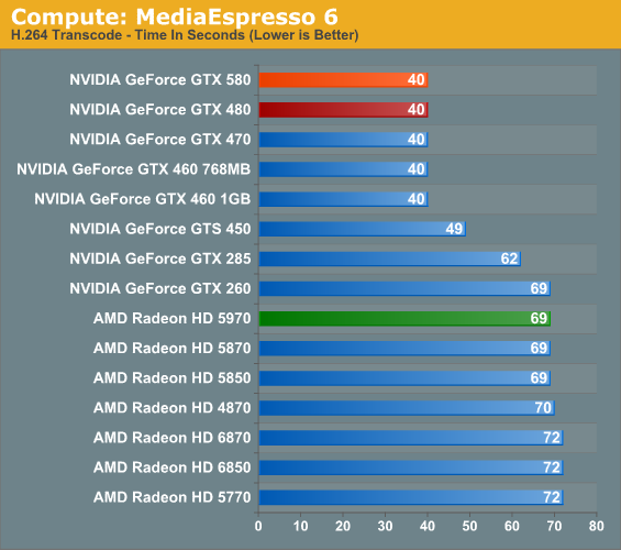
We throw MediaEspresso 6 in largely to showcase that not everything that’s GPU accelerated is GPU-bound, as ME6 showcases this nicely. Once we move away from sub-$150 GPUs, APIs and architecture become much more important than raw speed. The 580 is unable to differentiate itself from the 480 as a result.
Our third GPU compute benchmark is SmallLuxGPU, the GPU ray tracing branch of the open source LuxRender renderer. While it’s still in beta, SmallLuxGPU recently hit a milestone by implementing a complete ray tracing engine in OpenCL, allowing them to fully offload the process to the GPU. It’s this ray tracing engine we’re testing.
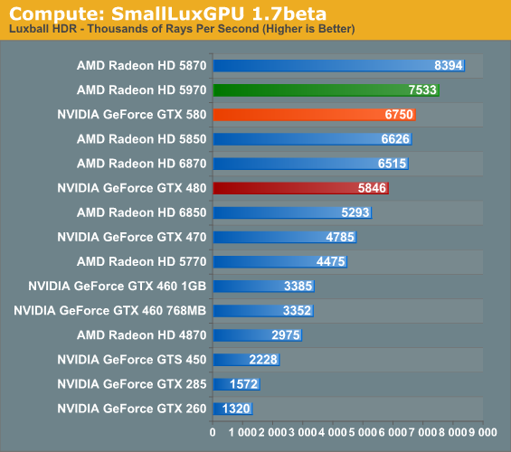
SmallLuxGPU is rather straightforward in its requirements: compute and lots of it. The GTX 580 attains most of its theoretical performance improvement here, coming in at a bit over 15% over the GTX 480. It does get bested by a couple of AMD’s GPUs however, a showcase of where AMD’s theoretical performance advantage in compute isn’t so theoretical.
Our final compute benchmark is a Folding @ Home benchmark. Given NVIDIA’s focus on compute for Fermi and in particular GF110 and GF100, cards such as the GTX 580 can be particularly interesting for distributed computing enthusiasts, who are usually looking for the fastest card in the coolest package. This benchmark is from the original GTX 480 launch, so this is likely the last time we’ll use it.
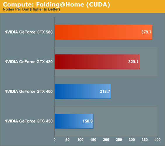
If I said the GTX 580 was 15% faster, would anyone be shocked? So long as we’re not CPU bound it seems, the GTX 580 is 15% faster through all of our compute benchmarks. This coupled with the GTX 580’s cooler/quieter design should make the card a very big deal for distributed computing enthusiasts.
At the other end of the spectrum from GPU computing performance is GPU tessellation performance, used exclusively for graphical purposes. Here we’re interesting in things from a theoretical architectural perspective, using the Unigine Heaven benchmark and Microsoft’s DirectX 11 Detail Tessellation sample program to measure the tessellation performance of a few of our cards.
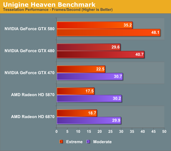
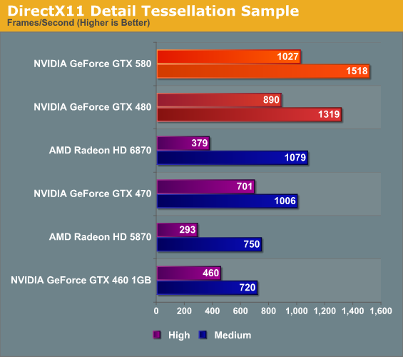
NVIDIA likes to heavily promote their tessellation performance advantage over AMD’s Cypress and Barts architectures, as it’s by far the single biggest difference between them and AMD. Not surprisingly the GTX 400/500 series does well here, and between those cards the GTX 580 enjoys a 15% advantage in the DX11 tessellation sample, while Heaven is a bit higher at 18% since Heaven is a full engine that can take advantage of the architectural improvements in GF110.
Seeing as how NVIDIA and AMD are still fighting about the importance of tessellation in both the company of developers and the public, these numbers shouldn’t be used as long range guidance. NVIDIA clearly has an advantage – getting developers to use additional tessellation in a meaningful manner is another matter entirely.
Power, Temperature, and Noise
Last but not least as always is our look at the power consumption, temperatures, and acoustics of the GTX 580. NVIDIA’s performance improvements were half of the GTX 580 story, and this is the other half.
Starting quickly with voltage, as we only have one card we can’t draw too much from what we know, but there are still some important nuggets. NVIDIA is still using multiple VIDs, so your mileage may vary. What’s clear from the start though is that NVIDIA’s operating voltages compared to the GTX 480 are higher for both idle and load. This is the biggest hint that leakage has been seriously dealt with, as low voltages are a common step to combat leakage. Even with these higher voltages running on a chip similar to GF100, overall power usage is still going to be lower. And on that note, while the voltages have changed the idle clocks have not; idle remains at 50.6MHz for the core.
| GeForce GTX 480/580 Voltages | |||||
| Ref 480 Load | Ref 480 Idle | Ref 580 Load | Ref 580 Idle | ||
| 0.959v | 0.875v | 1.037v | 0.962v | ||
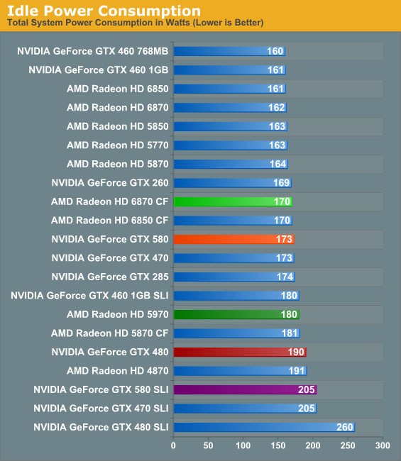
Beginning with idle power, we’re seeing our second biggest sign that NVIDIA has been tweaking things specifically to combat leakage. Idle power consumption has dropped by 17W on our test system even though the idle clocks are the same and the idle voltage higher. NVIDIA doesn’t provide an idle power specification, but based on neighboring cards idle power consumption can’t be far off from 30-35W. Amusingly it still ends up being more than the 6870 CF however, thanks to the combination of AMD’s smaller GPUs and ULPS power saving mode for the slave GPU.
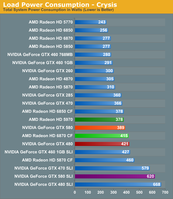
Looking at Crysis, we begin to see the full advantage of NVIDIA’s optimizations and where a single GPU is more advantageous over multiple GPUs. Compared to the GTX 480 NVIDIA’s power consumption is down 10% (never mind the 15% performance improvement), and power consumption comes in under all similar multi-GPU configurations. Interestingly the 5970 still draws less power here, a reminder that we’re still looking at cards near the peak of the PCIe specifications.
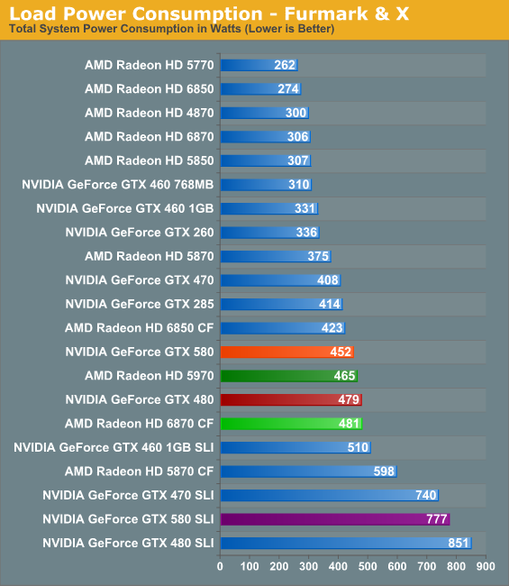
As for FurMark, due to NVIDIA’s power throttling we’ve had to get a bit creative. FurMark is throttled to the point where the GTX 580 registers 360W, thanks to a roughly 40% reduction in performance under FurMark. As a result for the GTX 580 we’ve swapped out FurMark for another program that generates a comparable load, Program X. At this point we’re going to decline to name the program, as should NVIDIA throttle it we may be hard pressed to determine if and when this happened.
In any case, under FurMark & X we can see that once again NVIDIA’s power consumption has dropped versus the GTX 480, this time by 27W or around 6%. NVIDIA’s worst case scenario has notably improved, and in the process the GTX 580 is back under the Radeon HD 5970 in terms of power consumption. Thus it goes without saying that while NVIDIA has definitely improved power consumption, the GTX 580 is still a large, power hungry GPU.
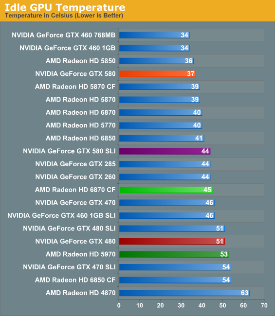
With NVIDIA’s improvements in cooling and in idle power consumption, there’s not a result more dramatic than idle GPU temperatures. The GTX 580 isn’t just cooler, it’s cool period. 37C is one of the best results out of any of our midrange and high-end GPUs, and is a massive departure from the GTX 480 which was at least warm all the time. As we’ll see however, this kind of an idle temperature does come with a small price.
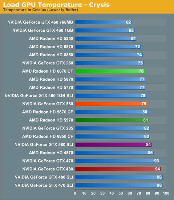
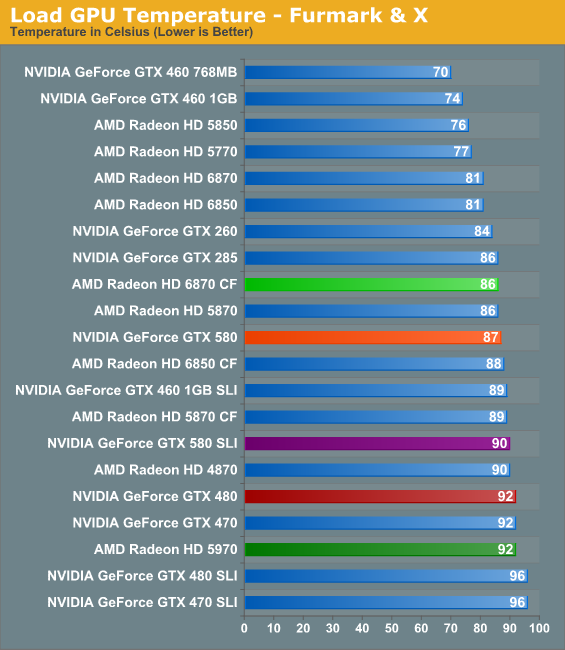
The story under load is much the same as idle: compared to the GTX 480 the GTX 580’s temperatures have dramatically dropped. At 79C it’s in the middle of the pack, beating a number of single and multi GPU setups, and really only losing to mainstream-class GPUs and the 6870 CF. While we’ve always worried about the GTX 480 at its load temperatures, the GTX 580 leaves us with no such concerns.
Meanwhile under FurMark and Program X, the gap has closed, though the GTX 580 remains in the middle of the pack. 87C is certainly toasty, but it’s still well below the thermal threshold and below the point where we’d be worried about it. Interestingly however, the GTX 580 is actually just a bit closer to its thermal threshold than the GTX 480 is; NVIDIA rated the 480 for 105C, while the 580 is rated for 97C. We’d like to say this vindicates our concerns about the GTX 480’s temperatures, but it’s more likely that this is a result of the transistors NVIDIA is using.
It’s also worth noting that NVIDIA seems to have done away with the delayed fan ramp-up found on the GTX 480. The fan ramping on the GTX 580 is as near as we can tell much more traditional, with the fan immediately ramping up with higher temperatures. For the purposes of our tests, this keeps the temperatures from spiking as badly.
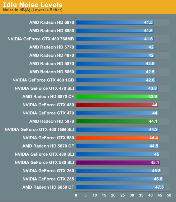
Remember where we said there was a small price to pay for such low idle temperatures? This is it. At 44.4dB, the 580 is ever so slightly (and we do mean slightly) louder than the GTX 480; it also ends up being a bit louder than the 5970 or 6870CF. 44.4 is not by any means loud, but if you want a card that’s whisper silent at idle, the GTX 580 isn’t going to be able to deliver.
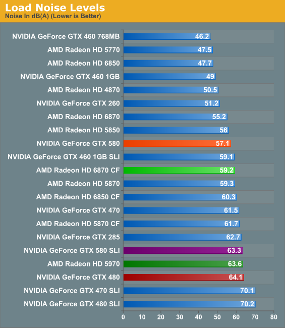
And last but not least is load noise. Between their improvements to power consumption and to cooling, NVIDIA put a lot of effort in to the amount of noise the GTX 580 generates. Where the GTX 480 set new records for a single GPU card, the GTX 580 is quieter than the GTX 285, the GTX 470, and even the Radeon HD 5870. In fact it’s only a dB off of the 5850, a card under most circumstances we’d call the epitome of balance between performance and noise. Graphs alone cannot demonstrate just how much of a difference there is between the GTX 480 and GTX 580 – the GTX 580 is not whisper quiet, but at no point in our testing did it ever get “loud”. It’s a truly remarkable difference; albeit one that comes at the price of pointing out just how lousy the GTX 480 was.
Often the mark of a good card is a balance between power, temperature, and noise, and NVIDIA seems to have finally found their mark. As the GTX 580 is a high end card the power consumption is still high, but it’s no longer the abnormality that was the GTX 480. Meanwhile GPU temperatures have left our self-proclaimed danger zone, and yet at the same time the GTX 580 has become a much quieter card under load than the GTX 480. If you had asked us in what NVIDIA needed to work on with the GTX 480, we would have said noise, temperature, and power consumption in that order; the GTX 580 delivers on just what we would have wanted.
Final Thoughts
Even though NVIDIA is only launching a single card today there’s a lot to digest, so let’s get to it.
Since the GeForce GTX 580 arrived in our hands last week, we’ve been mulling over how to approach it. It boils down to two schools of thought: 1) Do we praise NVIDIA for delivering a high performance single GPU card that strikes the right balance of performance and temperature/noise, or 2) Do we give an indifferent thumbs-up to NVIDIA for only finally delivering the card that we believe the GTX 480 should have been.
The answer we’ve decided is one of mild, but well earned praise. The GTX 580 is not the true next-generation successor to the GTX 480; it’s the GTX 480 having gone back in the womb for 7 months of development. Much like AMD, NVIDIA faced a situation where they were going to do a new product without a die shrink, and had limited options as a result. NVIDIA chose wisely, and came back with a card that is both decently faster and a refined GTX 480 at the same time.
With the GTX 480 we could recognize it as being the fastest single GPU card on the market, but only by recognizing the fact that it was hot and loud at the same time. For buyers the GTX 480 was a tradeoff product – sure it’s fast, but is it too hot/too loud for me? The GTX 580 requires no such tradeoff. We can never lose sight of the fact that it’s a high-end card and is going to be more power hungry, louder, and hotter than many other cards on the market, but it’s not the awkward card that the GTX 480 was. For these reasons our endorsement of the GTX 580 is much more straightforward, at least as long as we make it clear that GTX 580 is less an upgrade for GTX 480, and more a better upgrade for the GTX 285 and similar last-generation cards.
What we’re left with today is something much closer to the “traditional” state of the GPU market: NVIDIA has the world’s fastest single-GPU card, while AMD is currently nipping at their heels with multi-GPU products. Both the Radeon HD 5970 and Radeon HD 6870 CF are worthy competitors to the GTX 580 – they’re faster and in the case of the 6870 CF largely comparable in terms of power/temperature/noise. If you have a board capable of supporting a pair of 6870s and don’t mind the extra power it’s hard to go wrong, but only if you’re willing to put up with the limitations of a multi-GPU setup. It’s a very personal choice – we’d be willing to trade the performance for the simplicity of avoiding a multi-GPU setup, but we can’t speak for everyone.
So what’s next? A few different things. From the NVIDIA camp, NVIDIA is promising a quick launch of the rest of the GeForce 500 series. Given the short development cycles for NVIDIA we’d expect more refined GF10x parts, but this is very much a shot in the dark. Much more likely is a 3GB GTX 580, seeing as how NVIDIA's official product literature calls the GTX 580 the "GeForce GTX 580 1.5GB", a distinction that was never made for the GTX 480.
More interesting however will be what NVIDIA does with GF110 since it’s a more capable part than GF100 in every way. The GF100 based Quadros and Teslas were only launched in the last few months, but they’re already out of date. With NVIDIA’s power improvements in particular, this seems like a shoo-in for at least one improved Quadro and Tesla card. We also expect 500 series replacements for some of the GF100-based cards (with the GTX 465 likely going away permanently).
Meanwhile the AMD camp is gearing up for their own launches. The 6900 series is due to launch before the year is out, bringing with it AMD’s new Cayman GPU. There’s little we know or can say at this point, but as a part positioned above the 6800 series we’re certainly hoping for a slugfest. At $500 the GTX 580 is pricey (much like the GTX 480 before it), and while this isn’t unusual for the high-end market we wouldn’t mind seeing NVIDIA and AMD bring a high-intensity battle to the high-end, something that we’ve been sorely missing for the last year. Until we see the 6900 series we wouldn’t make any bets, but we can certainly look forward to it later this year.

