The NVIDIA Titan V Preview - Titanomachy: War of the Titans
by Ryan Smith & Nate Oh on December 20, 2017 11:30 AM ESTThe Volta Architecture: In Brief
Before we dive into our benchmark results, I want to spend a bit of time discussing the Volta architecture and the GV100 GPU in particular. Understanding what Volta brings to the table is critical for understanding the performance possibilities of the card, and understanding the GV100 GPU is similarly important for understanding the practical performance of the card.
Volta is a brand new architecture for NVIDIA in almost every sense of the word. While the logical organization is the same much of the time, it's not Pascal at 12nm with Tensor Cores. Rather it's a significantly different architecture in terms of thread execution, thread scheduling, core layout, memory controllers, ISA, and more. And these are just the things NVIDIA is willing to talk about right now, never mind the ample secrets they still keep.
Of the many architectural changes that Volta makes, there are four items in particular that I feel really set it apart from Pascal and help shape its capabilities.
- New tensor cores
- Removing the second warp scheduler dispatch unit & eliminating superscalar execution
- Separating the Integer cores
- Finer-grained thread scheduling
NVIDIA's Big Bet: Tensor Cores
The big story here of course is the new tensor cores. While the Volta architecture has all the makings of a strong HPC architecture even in a traditional context, the specific massive performance numbers that NVIDIA quotes for the Titan V and other Volta cards has come from the use of these tensor cores.
Tensor Cores are a new type of core for Volta that can, at a high level, be thought of as a more rigid, less flexible (but still programmable) core geared specifically for tensor math operations. These cores are essentially a mass collection of ALUs for performing 4x4 Matrix operations; specifically a fused multiply add (A*B+C), multiplying two 4x4 FP16 matrices together, and then adding that result to an FP16 or FP32 4x4 matrix to generate a final 4x4 FP32 matrix. Tensor operations are common in certain types of workloads, but in particular neural networking training and execution (inferencing).
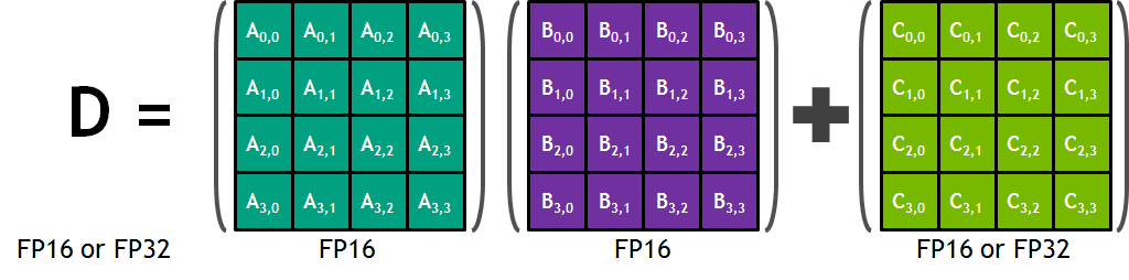
The significance of these cores are that by performing a massive matrix multiplication operation in one unit, NVIDIA can achieve a much higher number of FLOPS for this one operation. A single tensor core performs the equivalent of 64 FMA operations per clock (for 128 FLOPS total), and with GV100 packing 8 such cores per SM, results in 1024 FLOPS per clock per SM. By comparison, even with pure FP16 operations, the standard CUDA cores in a GV100 SM only generate 256 FLOPS per clock. So in scenarios where these cores can be used, we’re looking at the ability to hit 4x the performance versus Pascal.
The flip side to all of this is that the tensor cores are relatively rigid cores. They really aren’t very good for anything except tensor operations, so they are only applicable to certain classes of compute tasks, and right now I don’t know of any graphics tasks that would really benefit from the cores. The benefit to NVIDIA of doing this is that this allows the tensor cores to be very performance dense, both in total performance and in actual die space usage; by lumping together so many ALUs within a single core and without duplicating their control logic or other supporting hardware, the percentage of transistors in a core dedicated to ALUs is higher than on a standard CUDA core. The cost is flexibility, as the hardware to enable flexibility takes up space. So this is a very conscious tradeoff on NVIDIA’s part between flexibility and total throughput.
Meanwhile because tensor cores are brand-new to NVIDIA’s GPUs and because they need to be explicitly called upon, NVIDIA has a bit of a chicken & egg problem here. To make the most of the new hardware, NVIDIA needs developers to write software that taps into the new tensor cores, and in a roundabout way this is one of several roles the Titan V is designed to fill. The $3000 card is still expensive, but it’s the first workstation-class card incorporating these cores, vastly increasing the accessibility of the hardware to software developers. So whereas the first wave of Volta-optimized software has been specific big-ticket items like NVIDIA’s libraries and deep learning frameworks like Caffe2, Titan V will help developers put together the second wave of software.
Scheduling, ILP, & Integers
The second big change that Volta brings to the table is that, at least for GV100, the second warp scheduler dispatch port has been eliminated. Ever since GF104 in 2011, NVIDIA’s architectures have featured two dispatch ports per warp scheduler, allowing for superscalar execution. In other words, their architecture has relied on a degree of instruction level parallelism, requiring the ability to execute a second, non-dependent instruction from a thread in order to get the most out of the hardware.
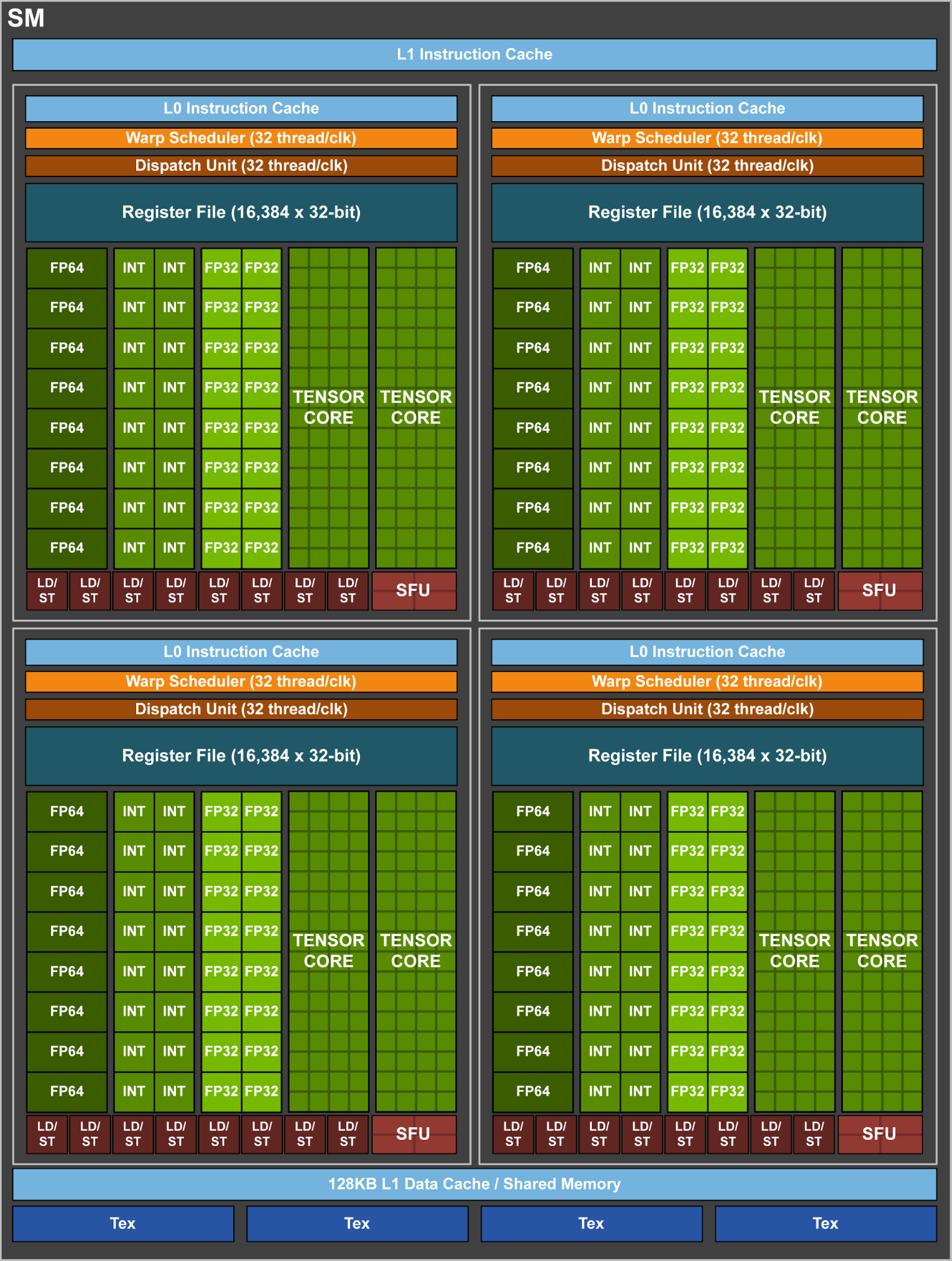
Volta/GV100, by contrast, is no longer superscalar. Each partition within an SM is now feed by a single dispatch unit warp scheduler, with no opportunity to extract ILP. This means that Volta is a pure thread level parallelism (TLP) design: max utilization comes from maximizing the number of threads active at any given time.
ILP versus TLP is a constant balance, and it’s not unusual to see NVIDIA shifting between the two, especially for a compute-centric GPU like GV100. ILP is nice to have, but extracting it can be difficult. On the other hand while GPUs are meant for embarrassingly parallel tasks, it’s not always easy to generate more threads. So there’s a very real question over whether the performance gains from adding the hardware for ILP justifies the power and complexity costs of doing so.
Meanwhile NVIDIA has also made an interesting change to the Volta architecture with respect to how the integer ALUs are organized. Though not typically a subject of conversation in NVIDIA architecture design, the integer ALUs have traditionally been paired with the FP32 ALUs to make up a single CUDA core. So a black of CUDA cores could either execute integer or floating point operations, but not both at the same time.
Volta in turn separates these ALUs. The integer units have now graduated their own set of dedicates cores within the GPU design, meaning that they can be used alongside the FP32 cores much more freely. The specifics of this arrangement get a bit hairy in light of the fact that Volta isn’t superscalar – so you technically can’t issue INT and FP32 instructions at the same time regardless – but given the fact that most GPU operations take multiple clocks to execute, this allows for much more flexibility than before. NVIDIA notes that it’s especially useful for address generation and in FMA performance, the latter of which we’re taking a look at a bit later.
Finally, and admittedly getting into the even more esoteric aspects of GPU design, NVIDIA has reworked how SIMT works for Volta. The individual CUDA cores within a 32-thread warp now have a limited degree of autonomy; threads can now be synchronized at a fine-grain level, and while the SIMT paradigm is still alive and well, it means greater overall efficiency. Importantly, individual threads can now yield, and then be rescheduled together. This also means that a limited amount of scheduling hardware is back in NV’s GPUs.
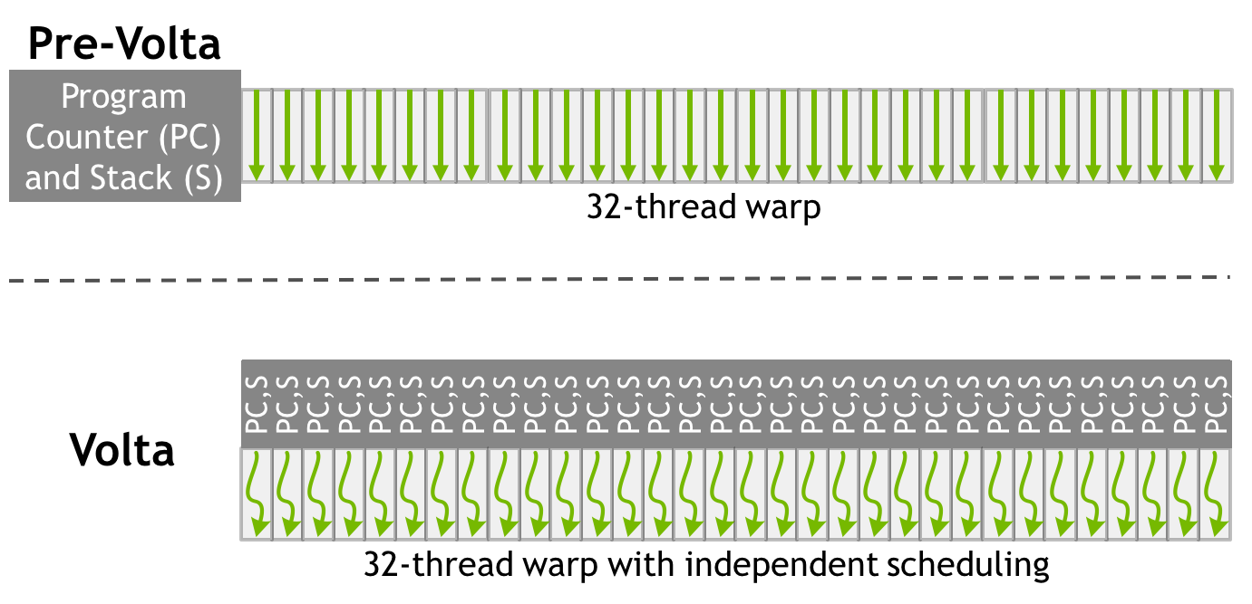
This generally doesn’t mean anything for existing software. But for developers who really know their GPUs and threading, it gives them ways to extract performance that couldn’t be done under Pascal’s more rigid SIMT model.


111 Comments
View All Comments
jjj - Wednesday, December 20, 2017 - link
Bah but this is last week's Titan, aren't they launching a new one this week?WorldWithoutMadness - Thursday, December 21, 2017 - link
Titan A, next week Titan G, next 2 weeks Titan I, next month Titan N, and lastly Titan ASshowster - Saturday, December 23, 2017 - link
*Slow Clap*Luscious - Wednesday, December 27, 2017 - link
Don't forget the dual Volta Titan ZZmode_13h - Wednesday, December 27, 2017 - link
...in case anyone wondered why they never released Pascal as Titan P. I guess Nvidia knows their market too well for that.mode_13h - Wednesday, December 27, 2017 - link
Well, they'll presumably release the GV102 in some more affordable flavor of Titan. Titan V0?And maybe they'll eventually release a GV100 in a PCIe card with all four HBM2 stacks... although that'll probably receive Quadro branding & price point, like the Quadro GP100.
mode_13h - Tuesday, January 30, 2018 - link
So, after Titan Xp and Titan V(ista), next should be Titan 7. That's a definite buy, but I'd skip Titan 8. Maybe go for Titan 8.1, or just hold out for Titan 10.CajunArson - Wednesday, December 20, 2017 - link
OK, while I agree that nobody should buy a Titan V for gaming you say: "Already after Battlefield 1 (DX11) and Ashes (DX12), we can see that Titan V is not a monster gaming card, though it still is faster than Titan Xp. "Uh... yeah that's wrong. Anything that's faster than a Titan XP *is* a monster gaming card by definition. It's just not a very good purchase for $3000 since it's not really targeted towards gaming.
nathanddrews - Wednesday, December 20, 2017 - link
I agree with this. Cost aside - it's the best gaming card on the market. Unless NVIDIA launches the 1180/2080/whatever80 soon, this card will be in Terry Crews' Old Spice rig by the end of the month.P-P-P-POWWWWERRRRRRRRRR!
Ryan Smith - Wednesday, December 20, 2017 - link
"Uh... yeah that's wrong. Anything that's faster than a Titan XP *is* a monster gaming card by definition."The big issue right now is that it's not consistently faster, especially at the 99th percentile Or for that matter, not as bug-free as it needs to be.
I'm going to be surprised if it doesn't get better with later drivers. But for the moment, even if you throw out the price, it's kind of janky in games.