Testing a Chinese x86 CPU: A Deep Dive into Zen-based Hygon Dhyana Processors
by Dr. Ian Cutress & Wendell Wilson on February 27, 2020 9:00 AM ESTHygon CPUs: Chinese Crypto, Different Performance
The big overriding question is about what exactly has changed with these processors compared to the standard Ryzen and EPYC CPUs. To say that they are rebadged processors, as some have suspected, is completely incorrect – we can tell this alone by the different cryptography engines provided by the Linux kernel updates. But we also detected other differences.
By and large, as we could determine, the core layout is identical, with the same cache sizes, TLB sizes, and port allocations – there were no differences at this fundamental level. The CPU still offered 64 KB 4-way for the L1 instruction cache, 32 KB 8-way for the L1 data cache, 512 KB 8-way for the L2 cache, and 8 MB 16-way for the L3 cache, identical to the Zen 1 core. TLB entries are as follows:
- L1D + L1I: 4K/2M/1G 64-entry
- L2D: 4K 1536-entry 6-way, 2M 1536-entry 3-way, no 1G
- L2I: 4K/2M 1024-entry 8-way, no 1G
Memory access times are 4 cycles for L1, 12 cycles for L2, and 37-40 cycles for L3. Memory latency was measured at 284-307 cycles.
L1 read speeds were measured around 32 bytes per clock (805 GB/s total, ~100 GB/s per core), while write speeds were measured around 16 bytes per clock (408 GB/s total, ~51 GB/s per core). DDR4 Memory speed for the 8-core gave 38.5 GB/s for reads and 35.8 GB/s for writes.
Cryptography Changes
For the cryptography changes, these are detailed in the Linux kernel updates. The updates revolve around AMD’s secure encryption for virtualization features, or SEV. Normally with an EPYC processor, SEV is governed by the cryptography protocols defined by AMD, in this case RSA, ECDSA, ECDH, SHA, and AES. In order to generate the right keys, SEV uses these methods. However, in the Hygon Dhyana designs, SEV is built to use algorithms known as SM2, SM3, and SM4.
As stated in the updates, SM2 is based on elliptic curve cryptography, and requires additional private/public key exchange. SM3 is a hashing algorithm, similar to SHA-256, and SM4 is a block cipher algorithm, similar to AES-128. Additional commands are placed into the Linux kernel in order to support the extra functions these algorithms need. In the notes it states that these algorithms were successfully tested on Hygon Dhyana Plus (presumably the big CPU) processors but they were also successfully tested on AMD’s EPYC CPUs.
Slowing Down Some Instructions
The biggest update to the design we were able to determine is in the instruction throughput. We don’t think that this difference between Dhyana Plus and EPYC has been mentioned before, and we did extra checks to make sure our software was displaying the right data, but put simply some instructions have been purposefully made slower. This has some rather serious implications, especially depending on when it occurred in the pipeline.
What we think is the case is that in order for AMD to export its SoC design, it had to also share microcode relating to how the CPU interprets instructions, and it was told to slow down certain key instructions (or disable them altogether) in order to make the arrangement with the joint venture and China work.
In our testing, we found that while integer performance is similar between Hygon and EPYC, certain floating point instructions, namely DIV and SQRT, are not pipelined in the Hygon CPU. This means throughput and latency is reduced. A lot of simple MMX/SSE instructions have reduced throughput:
| Instruction Throughput Differences | ||
| AnandTech | EPYC Naples |
Hygon Dhyana |
| ADD/SUB | 2 per clock | 1 per clock |
| CMP/MULP* | 2 per clock | 1 per clock |
| ADDSUBP* | 2 per clock | 1 per clock |
| RCP*/RSQRT* | 1 per clock | 0.5 per clock |
| BLENDW | 3 per clock | 2 per clock |
| PMIN/MAX* | 3 per clock | 2 per clcok |
| PAND/ANDN/OR/XOR | 4 per clock | 2 per clock |
| MOVs | 4 per clock | 2 per clock |
All of these instructions are pretty important for even basic tasks. By limiting the simultaneous throughput of these instructions, it means that these CPUs cannot compute code that can be parallelized as fast, ultimately decreasing performance.
Perhaps the biggest change however was one that even differed between the server ‘Dhyana Plus’ processor and the consumer ‘Dhyana’ version. Random number generation, which is a key backbone in a lot of stochastic and financial processes, is severely reduced on the Dhyana Plus. The key instructions, RDRAND and RDSEED, have various reasons for being slow/fast. Here’s the comparison:
| Instruction Latency Differences | |||
| AnandTech | Zen 1 Desktop |
Hygon Dhyana |
Hygon Dhyana Plus |
| RDRAND | |||
| 16-bit | 1200 clocks | 1100 clocks | 800 clocks |
| 32-bit | 1200 clocks | 1100 clocks | 800 clocks |
| 64-bit | 2365 clocks | 2125 clocks | 1520 clocks |
| RDSEED | |||
| 16-bit | 1200 clocks | 1100 clocks | 12000 clocks |
| 32-bit | 1200 clocks | 1100 clocks | 12000 clocks |
| 64-bit | 2365 clocks | 2125 clocks | 27100 clocks |
That’s quite a difference, especially in RDSEED. We saw that RDSEED, the seed generation to help spawn random number algorithms, is over 10x slower on the server chip, and RDRAND, used for actually generating hardware based random numbers, is faster than standard Ryzen – moreso on the server chip. Interestingly enough, the same delays for RDSEED for the server chips are also seen on Ryzen Mobile and Ryzen Desktop APUs.
For RDRAND, having a faster random number generator can be indicative of two things: either it is actually faster, or the random algorithm has a lower periodicity, i.e. the point at which an algorithm wraps on itself. The best pseudo-RNG have the largest periodicity, so in this case the RDRAND is fast leads us to conclude that the periodicity is low, leading to lower quality random numbers.
For RDSEED, the fact that this is 10x slower is a little different. RDSEED is meant to take information from the various sensors on board and output a random value to initialize the RDRAND – it should only get called once per periodicity. A slower RDSEED either means its taking data from more sources (a good thing), or it’s being slowed down on purpose (a bad thing).
In actual fact, RDRAND and RDSEED can be enabled/disabled in the BIOS of our Dhyana Plus system.
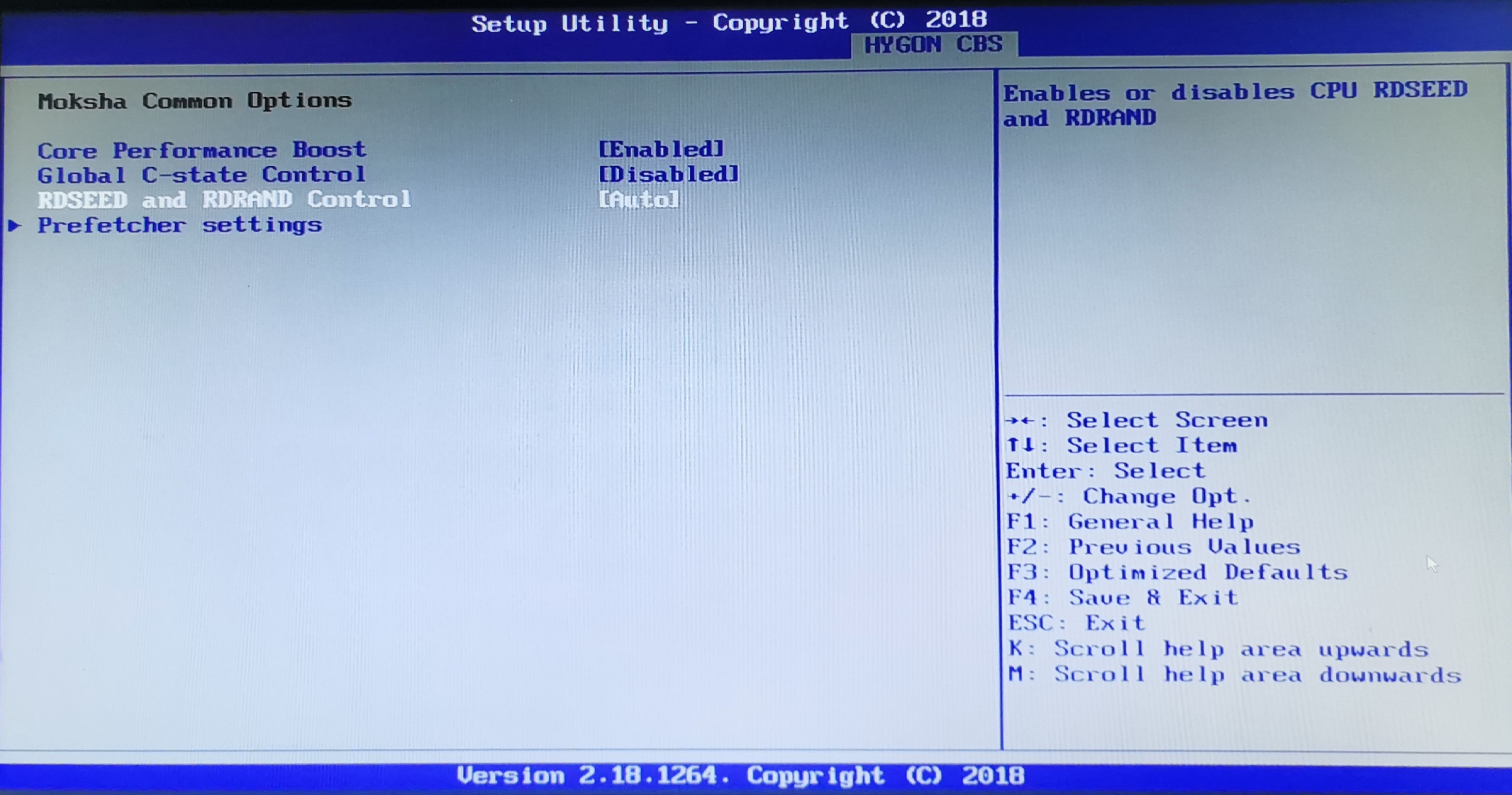
It’s amusing that this menu is called ‘Moksha Common Options’. Moksha being a word commonly associated with ‘enlightenment’ or ‘release’. This is either a clever word play, or someone digging out a non-contextual old Chinese to English dictionary in translation.
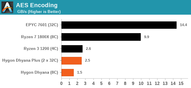
When it comes to AVX and AVX2 performance, even though the CPUs were able to identify themselves as having AVX and AVX2 support, trying to actually measure these instructions failed – in our instruction dumps, they were listed as ‘supported, disabled’. When it comes to supported features, Zen 1 typically lists AESNI, SHA, CLMUL, FMA4, BMI and BMI2 as supported instructions - none of these instructions are supported on the Hygon CPUs.
For things like AES, we have a direct benchmark for these, and the fact that these CPUs do not support AES means that we get a tanking in performance:
It should also be noted that the typical methods for finding the power consumption on AMD CPUs by probing registers also failed here. These seem to be removed from the CPU altogether.


133 Comments
View All Comments
ingwe - Thursday, February 27, 2020 - link
Interesting and cool that you were able to test it! This is definitely one of the reasons why I come to anandtech.sandtitz - Thursday, February 27, 2020 - link
"if you find anything out, we may confirm it"Ian, did you ask AMD for confirmation then?
romrunning - Thursday, February 27, 2020 - link
I'm sure Marvel regrets selling rights to the X-Men & Spiderman to the various studios for the cash infusion. I wonder if AMD will similarly regret this, when more cash & resources come from "outside" sources to THATIC & the Hygon CPUs significantly improves over their initial Zen "licensing" deal.ArcadeEngineer - Thursday, February 27, 2020 - link
How? The IP they got is for a GloFo manufacturing process, and GloFo are no longer able to deal with them. These weren't being produced in China, at least at the die level.romrunning - Thursday, February 27, 2020 - link
I was thinking if Hygon begins to improve and then eclipses AMD's own Ryzen/EPYC CPUs. Basically, you may have enabled a future competitor to jump over years/decades of in-house design with an initial starting design that would has a lot of advancements from the beginning. I'm sure it would still take years, but you would think that having one main competitor (Intel) is better than having 3-4.FreckledTrout - Thursday, February 27, 2020 - link
Possible but very unlikely. Especially seeing who this IP went to and there lack of innovation and creativity.Stuka87 - Thursday, February 27, 2020 - link
I am sure there is some pretty specific text in the agreement that very much limits what Hygon can and cannot do with the design.Holliday75 - Thursday, February 27, 2020 - link
Yeah its not like China is known for IP theft and producing counterfeit products the world over.Retycint - Thursday, February 27, 2020 - link
This is the x86 IP we're talking about here, and I wager this agreement is going to be taken a lot more seriously than some random startup's patentNotmyusualid - Sunday, March 1, 2020 - link
@Retycint - Explain to me how you sue a Chinese company in the USA...should they fall foul of any 'agreements'. Remember the copied X5? I saw one with my own eyes - and have owned one - it was dead on copy. BMW lost that one in a Chinese court.