AMD Reveals The Radeon RX 6000 Series: RDNA2 Starts At The High-End, Coming November 18th
by Ryan Smith on October 28, 2020 12:25 PM EST- Posted in
- GPUs
- AMD
- Radeon
- RDNA2
- RX 6000 Series
- RX 6800 XT
RDNA2 At A High Level: Ray Tracing, Infinity Cache, & A Whole Lot of Clockspeed
Underpinning virtually everything that AMD wants to accomplish with their new RX 6000 series cards will be the RDNA2 GPU architecture. Not to harp on this point more than is necessary, but it needs to be underscored that AMD doesn’t get the benefit of a new process node for the RX 6000 series cards; the company will be using the same TSMC 7nm process that they used for RX 5000 family. So almost everything AMD gets out of the new parts performance-wise is going to come from architectural improvements. And architectural improvements are not easy to come by.
Ever since AMD announced the RDNA2 architecture, they have reiterated a singular goal: they wanted to achieve a 50% jump in perf-per-watt over RDNA1. And that they would accomplish it entirely with architectural improvements, not process improvements.
To put it diplomatically, this is a tall order, especially for AMD. RDNA (1), even with its complete replumbing of AMD’s core GPU architecture and the benefit of the move to TMSC’s 7nm node only achieved a bit more than a 50% improvement. And now AMD has to do the same thing only a bit over a year later, without a new manufacturing node? These kinds of major leaps have been done before – most famously with NVIDIA’s Maxwell architecture – but they are few and far between, as they are very hard to pull off.
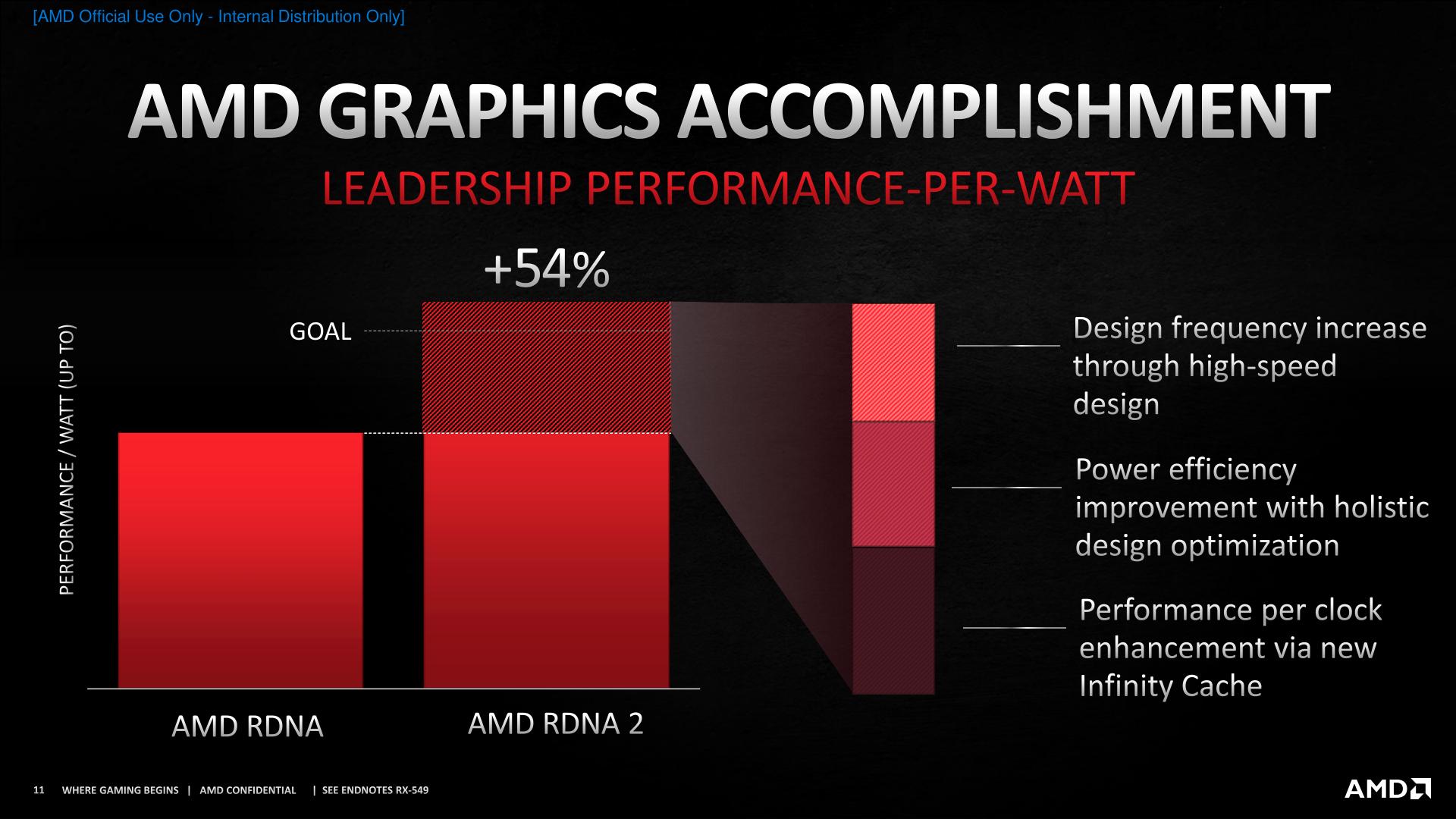
But pull it off AMD has, according to today’s keynote. The company is touting that RDNA2 offers a 54% perf-per-watt increase over RDNA (1) thanks to the combined efforts of their enhancements. We will obviously be testing AMD’s RX 6000 series cards in great detail in the coming weeks to confirm whether this is true, but taking AMD at face value here, if this is true, then it’s a major accomplishment on their end.
AMD will disclose more about RDNA2 and its optimizations later on in their full tech deep dives, but for today there are offering a high-level overview focusing on the three big sources of efficiency gains for RDNA2: more energy-efficient CUs, higher frequencies at the same power levels, and an increase in real-world perf-per-clock/IPC thanks to the Infinity Cache.
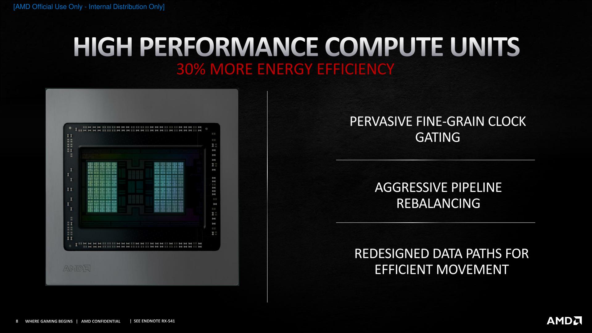
Starting with the CUs, RDNA2 incorporates a revised CU design that has undergone extensive power management upgrades. According to AMD they’re not only doing more fine-grained clock gating than ever before to eliminate energy wastage, but they have reworked the CU’s data paths as well to reduce energy spent there. This is a more important change than it would first appear, as the costs of moving data, rather than just processing it, are quickly becoming a major energy burden. Shuffling bits in and out of VRAM is very expensive, and even sending them elsewhere in the chip has a cost. So minimizing the amount of energy spent on moving data is a core optimization strategy for ASICs in this day and age.
AMD’s presentation also quickly talked about aggressive pipeline rebalancing, though the company isn’t disclosing any more details than that. For the moment, I’m assuming that the core architecture hasn’t seen any significant changes – that each CU still contains two SIMD32 units – but AMD may have made some smaller changes around that. So we’ll have to see what AMD tells us over the coming weeks.
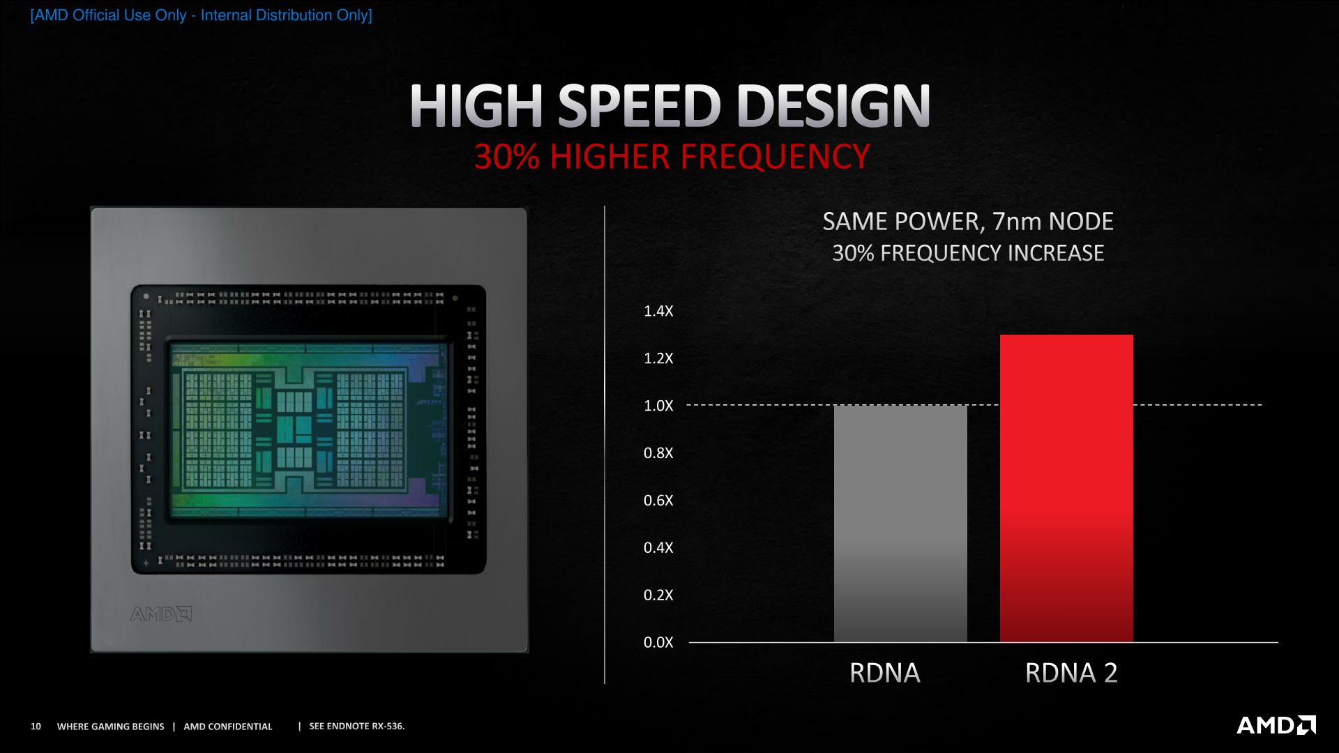
Going hand-in-hand with the energy optimizations to the CUs, AMD has also done chip-wide optimizations to improve on how high they can clock their silicon, and the power costs of those high frequencies. So if you’ve been wondering how Sony is able to get the PS5’s iGPU up to 2.2GHz+, we’re about to see just how that’s been done on the RX 6000, as AMD has implemented similar changes here. Overall AMD is claiming that they can clock 30% higher at the same power, which that alone would deliver a lot of AMD’s claimed 54% improvement in perf-per-watt over RDNA (1). AMD has previously talked about how their experiences with the Zen architecture have guided their GPU efforts as well, and this is an area in particular where their Zen learnings have been very applicable.
Infinity Cache

Last, but not least, we have the mysterious Infinity Cache. AMD is not going into too many details about the Infinity Cache today, but at a high level, this is a sizable on-chip cache that according to AMD functions a lot like an L3 cache on a CPU. Just how similar remains to be seen, but conceptually, it can be thought of as a local cache that buffers against reads and writes to the main memory, and provides a backstop for large operations that’s a lot faster than having to go out to VRAM.
On-chip caches for GPU usage are not a new idea, especially for AMD. The company included a 32MB eSRAM cache for the Xbox One (and Xbox One S) SoC, and even before that the Xbox 360 had an on-package eDRAM as well. But this is the first time we’ve seen a large cache on a PC GPU.
Navi 21 will have a 128MB Infinity Cache. Meanwhile AMD isn’t speaking about other GPUs, but those will presumably include smaller caches as fast caches eat up a lot of die space.
On that note, let's talk about the size of the infinity Cache. In short, based on currently available data it would appear that AMD has dedicated a surprisingly large portion of their transistor budget to it. Doing some quick paper napkin math and assuming AMD is using standard 6T SRAM, Navi 21’s Infinity Cache would be at least 6 billion transistors in size, which is a significant number of transistors even on TSMC’s 7nm process (for reference, the entirety of Navi 10 is 10.3B transistors). In practice I suspect AMD has some optimizations in place to minimize the number of transistors used and space occupied, but regardless, the amount of die space they have to be devoting to the Infinity Cache is significant. So this is a major architectural trade-off for the company.
But AMD isn't just spending transistors on cache for the sake of it; there are several major advantages to having a large, on-chip cache, even in a GPU. As far as perf-per-watt goes, the cache further improves RDNA2’s energy efficiency by reducing the amount of traffic that has to go to energy-expensive VRAM. It also allows AMD to get away with a smaller memory subsystem with fewer DRAM chips and fewer memory controllers, reducing the power consumed there. Along these lines, AMD justifies the use of the cache in part by comparing the power costs of the cache versus a 384-bit memory bus configuration. Here a 256-bit bus with an Infinity Cache only consumes 90% of the power of a 384-bit solution, all the while delivering more than twice the peak bandwidth.
Furthermore, according to AMD the cache improves the amount of real-world work achieved per clock cycle on the GPU, presumably by allowing the GPU to more quickly fetch data rather than having to wait around for it to come in from VRAM. And finally, the Infinity Cache is also a big factor in AMD’s ray tracing accelerator cores, which keep parts of their significant BVH scene data in the cache.
Ultimately, today is just a teaser of sorts for the Infinity Cache. Besides the die space costs, there are numerous outstanding questions about performance, how the cache is used (can developers directly access it?), and how well it works with existing software. Dedicating so much of a GPU to a large, on-die cache/memory pool is arguably a risky decision – it should be noted that while Microsoft followed a similar strategy for the Xbox One, they went with a tried-and-true large GDDR memory bus for the Xbox One X – so I’m very curious how AMD is going to use a relatively small 128MB cache to make up for what would have otherwise been another 4GB+ of VRAM and 256GB/sec more VRAM bandwidth. Of everything AMD is doing today the Infinity Cache is the most revolutionary change, but it’s also the most questionable for a PC GPU.
Finally, it should be noted that as far as the Infinity Cache goes, AMD isn’t talking about the consoles either. While it’s billed as a central part of the RDNA2 architecture, it’s unclear at this time whether either console vendor opted to include it (even in a smaller form) for their respective devices. Both the PS5 and XSX come with significant DRAM subsystems, and neither console maker has talked about a large cache in their technical disclosures.
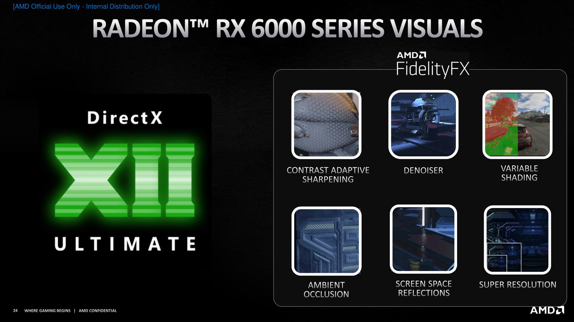
RDNA2 Features: Making The Jump To DirectX 12 Ultimate
Along with numerous optimizations to the power efficiency of their GPU architecture, RDNA2 also includes a much-needed update to the graphics side of AMD’s GPU architecture. RDNA (1), though a massive replumbing of the core compute architecture, did not include any graphics feature upgrades. As a result, AMD only offered a DirectX feature level 12_1 feature set – the same as the Radeon RX Vega series – at a time when NVIDIA was offering ray tracing and the other features that have since become DirectX 12 Ultimate (fl 12_2). So RDNA2 is AMD’s cache to catch up in features as well as performance, as they are integrating the latest and greatest in GPU graphics tech.
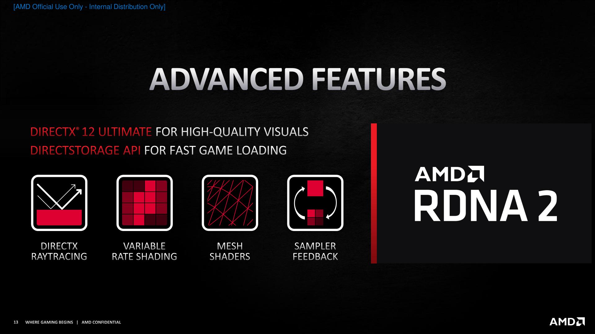
AMD has previously disclosed that RDNA2 would be a DX12 Ultimate-level architecture, so there aren’t much in the way of major reveals to be had here, nor will I recap DX12U in great depth.
Overall, DirectX 12 Ultimate focuses on 4 major features (and some minor spec changes): Ray tracing, tier 2 variable rate shading, mesh shaders, and sampler feedback. Ray tracing has received the most attention for obvious reasons, especially as NVIDIA has heavily promoted it. The rendering model based on how light bounces around in the real world can add a lot of detail with better lighting and reflections, but it is relatively expensive to use.
Meanwhile variable rate shading and mesh shaders are going to be less visible to end users, but they offer tangible performance improvements, and in the case of mesh shaders will eventually dramatically alter the geometry pipeline for games designed with mesh shaders as a baseline feature. Finally, sampler feedback will allow game developers to get a better idea of what textures and texel blocks within those textures are being used, allowing developers to better manage what assets are in VRAM and what needs to be pre-loaded.
Ray tracing itself does require additional functional hardware blocks, and AMD has confirmed for the first time that RDNA2 includes this hardware. Using what they are terming a ray accelerator, there is an accelerator in each CU. The ray accelerator in turn will be leaning on the Infinity Cache in order to improve its performance, by allowing the cache to help hold and manage the large amount of data that ray tracing requires, exploiting the cache’s high bandwidth while reducing the amount of data that goes to VRAM.
AMD is not offering any performance estimates at this time, or discussing in depth how these ray accelerators work. So that will be something else to look forward to once AMD offers deep dives on the technology.
Finally, AMD today is also confirming that they will offer support for Microsoft's DirecStorage API. Derived from tech going into the next-gen consoles, DirectStorage will allow game assets to be streamed directly from storage to GPUs, with the GPUs decompressing assets on their own. This bypasses the CPU, which under the current paradigm has to do the decompression and then send those decompressed assets to the GPU.
Platform Synergy: AMD Smart Access Memory
Besides fleshing out their feature capabilities at the hardware level in the RDNA2 architecture directly, as a CPU and GPU (and APU) maker, AMD has also been looking at how to leverage any possible synergy between their CPU and GPU platforms. And for their forthcoming Ryzen 5000 platforms, they’ve added a new trick to their toolkit when the Radeon RX 6000 is used with those new CPUs, in a feature AMD calls Smart Access Memory.
For the purposes of today’s keynote from AMD, the company is saying very little about the technology. From the bits and pieces that AMD has disclosed, the company has told me that the tech adjusts how data is transferred between the GPU and the CPU by giving the CPU direct access to the full 16GB of the GPU’s VRAM, avoiding the usual 256MB aperature limitation between CPUs and PCIe devices. The net result is that Smart Access Memory will be able to reduce memory fragmentation within the VRAM pool, which will improve performance.
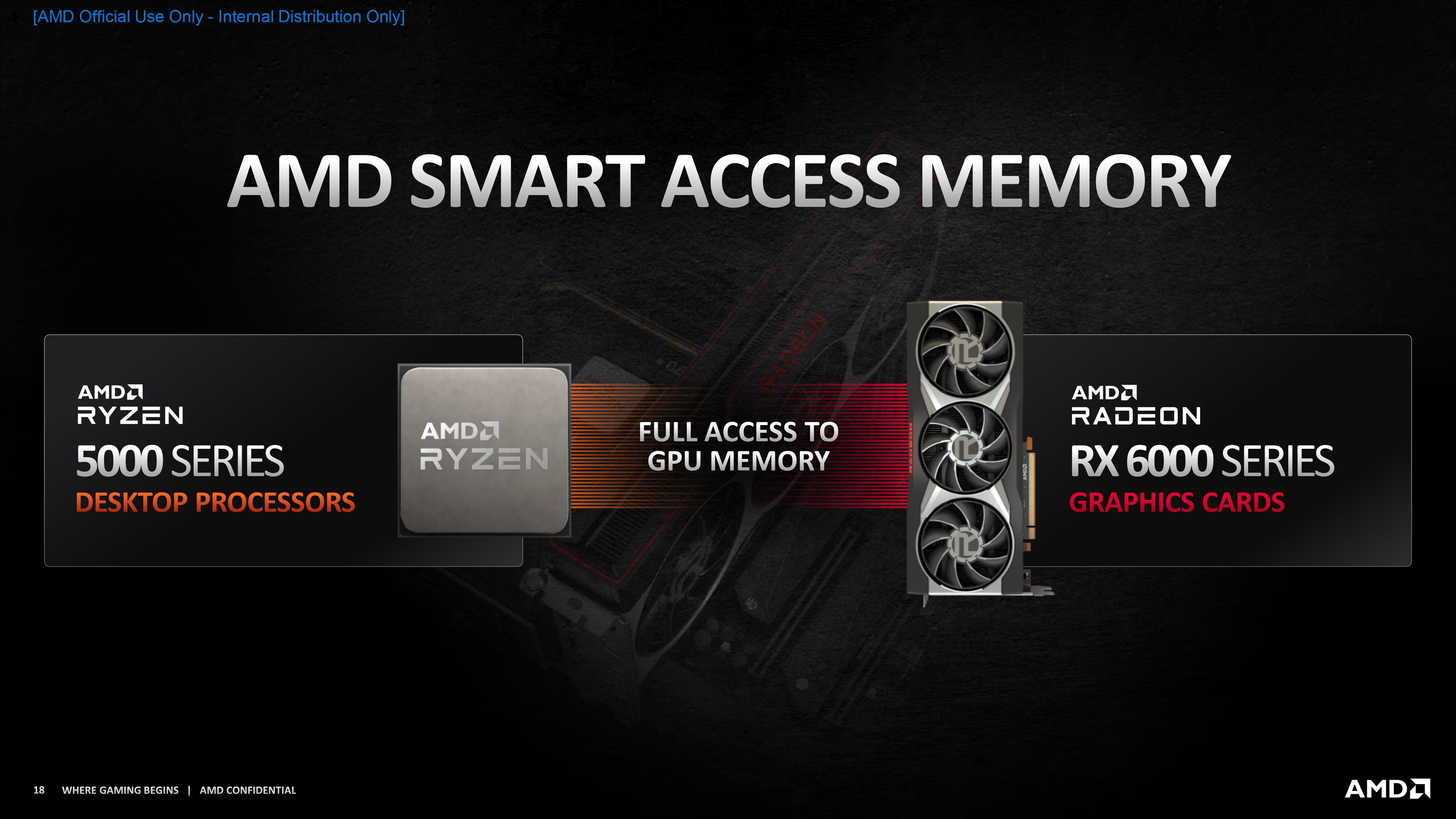
Meanwhile, Smart Access Memory will have a degree of automatic support to it. As things stand, many AAA games can use it today automatically and get some degree of a performance gain. But to get the best results, developers will still want to program games with the technology in mind.
Software Synergy: Rage Mode, Fidelity FX, & Super Resolution
Video cards as a whole have been platforms for some time; that is to say that it’s not just the hardware that matters, but software features count for something as well. Just ask NVIDIA, who has built large parts of their current graphics empire on this paradigm. AMD of course recognizes the need for software features as well, and for the RX 6000 series they’ll be rolling out some new software features to improve Radeon as a platform.
The marquee software addition here is what AMD is calling Rage Mode. This is a new, one-click automatic overclocking feature they are developing. In theory, a user can simply enable Rage Mode, let the computer do its thing to find the highest stable clockspeeds, and then enjoy the improved performance of their video card.
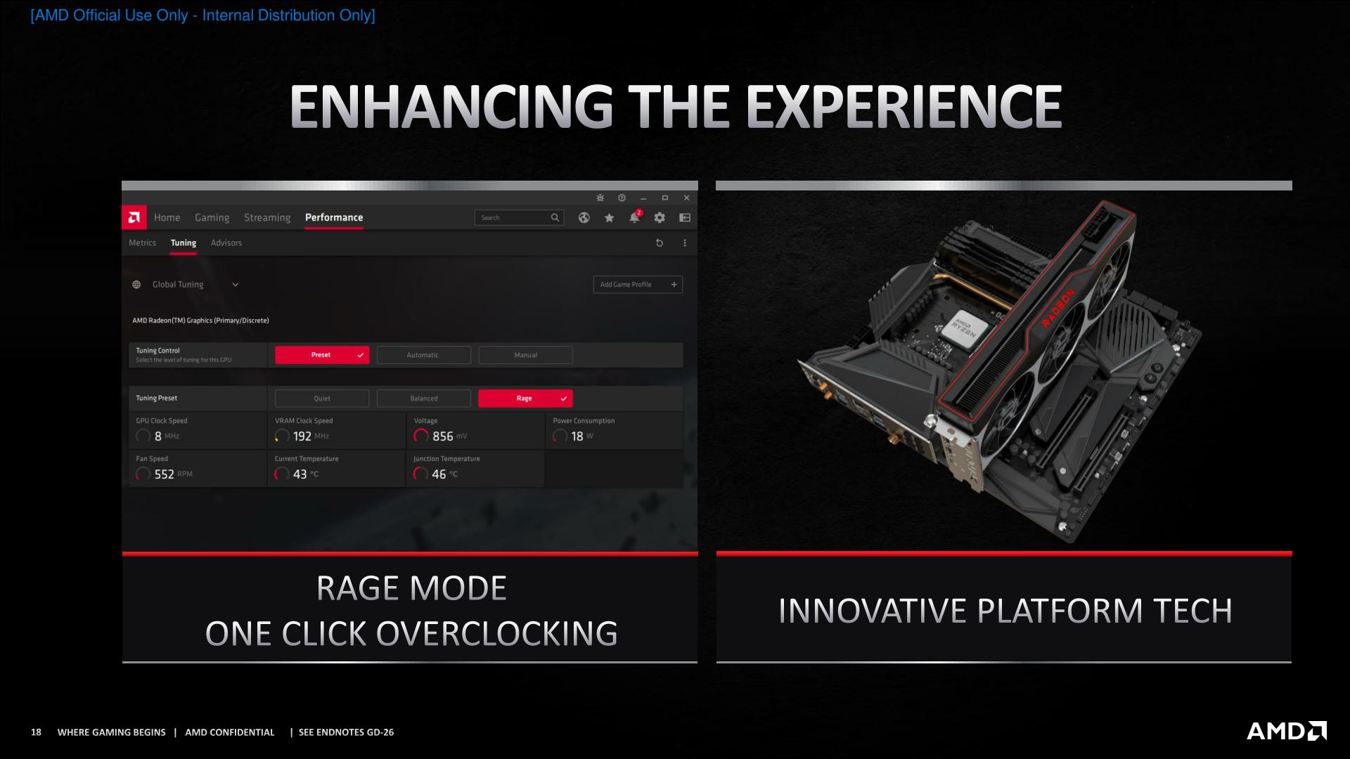
Automatic overclocking is not a new idea, even to AMD and its partners. So absent any further details on Rage Mode, I am curious how they’re implementing it and how they’re handling stability checks. Despite the one-click nature of automatic overclocking, I’ve found that previous implementations have had much higher friction in practice, especially when a system would crash during overclocking testing when it found an unstable GPU frequency. If AMD has a way to gracefully do this, that would greatly improve the experience, I believe.
Though regardless, users will need to keep in mind that any kind of one-click overclock stability testing will not be as rigorous as the stability testing done at the factory. So I don’t expect every last RX 6000 owner to use the feature, and I don’t expect it to put AMD’s partners out of business when it comes to factory overclocked video cards.
Meanwhile it should be noted that AMD has confirmed that Rage Mode is not warranty voiding. So users can still claim warranty coverage on their cards if they’ve used AMD’s official, user-friendly methods of overclocking.
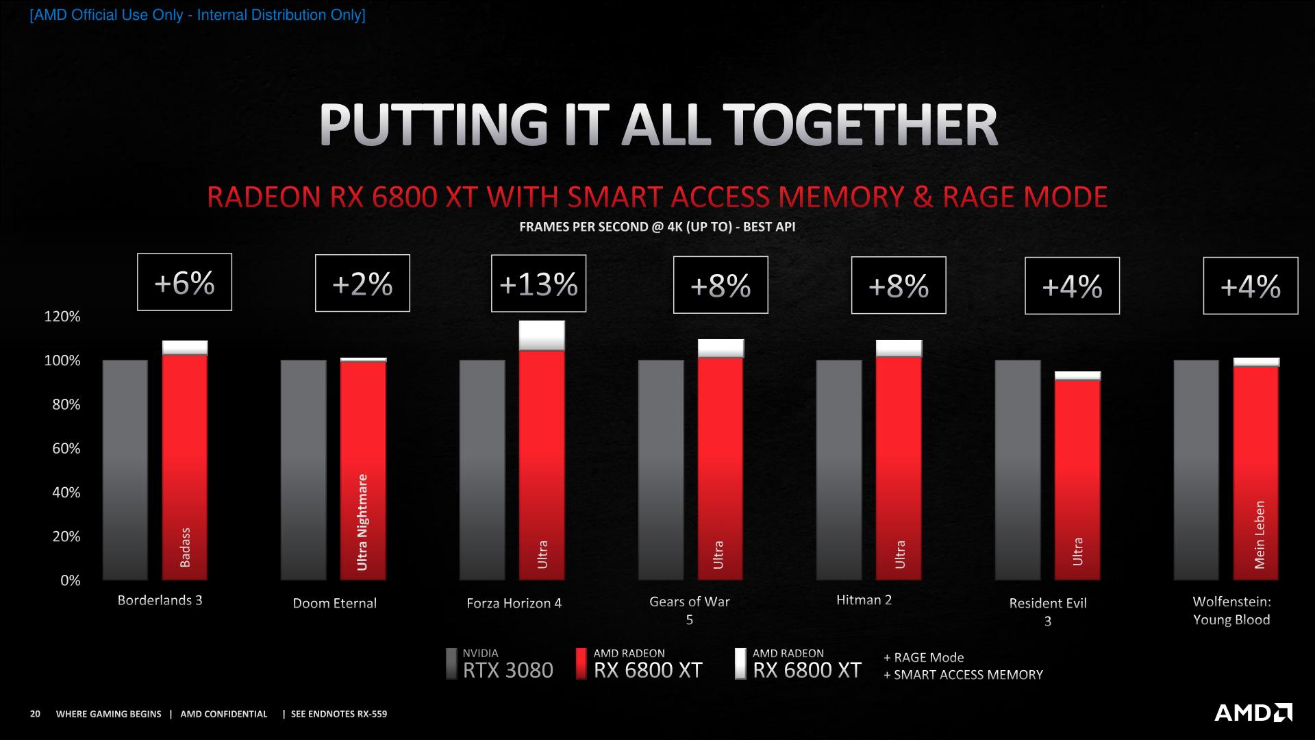
The performance gains from overclocking, in turn, will vary with chip and board quality. Some chips barely make spec, others fly past it; so overclocking is always subject to the silicon lottery. To that end, AMD Isn’t offering any specific performance claims with respect to Rage Mode, but they are publishing a slide showing a combination of gains in their testing from Rage Mode and Smart Access Memory.
AMD is also continuing to work on its FidelityFX suite of graphics libraries. Much of this is held over from AMD’s existing libraries and features, such as contrast adaptive sharpening, but AMD does have one notable addition in the works: Super Resolution.
Intended to be AMD’s answer to NVIDIA’s DLSS technology, Super Resolution is a similar intelligent upscaling technique that is designed to upscale lower resolution images to higher resolutions while retaining much of their sharpness and clarity. Like DLSS, don’t expect the resulting faux-detailed images to completely match the quality of a native, full-resolution image. However as DLSS has proven, a good upscaling solution can provide a reasonable middle ground in terms of performance and image quality.
As things currently stand super Resolution is still under development, so it won’t be available to game developers (or gamers) at the time of the RX 6000 series launch. But once it is, like AMD’s other FidelityFX graphics libraries, it will be released as an open source project on GPUOpen, and AMD is explicitly noting that it’s being designed as a cross-platform solution. Game devs will also be happy to hear that AMD is aiming to make it easier to implement across games than DLSS, which would make the tech more accessible and able to be implemented into a larger number of games.
Performance Claims and a Pinch of Salt
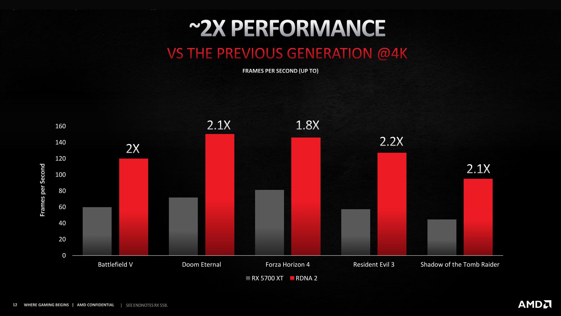
Finally, along with today’s announcement AMD has also published several slides with performance claims for the new parts. These slides primarily line things up against the NVIDIA competition, and like all unverified vendor results, should be taken with a grain of salt.
The big push in today’s announcement is of course the RX 6800 XT, and this is also where AMD’s claims are the most apples-to-apples. As it turns out, it was the 6800 XT that AMD was using when they offered a GPU performance teaser earlier this month. And the rest of the numbers from AMD’s lineup look quite similar.
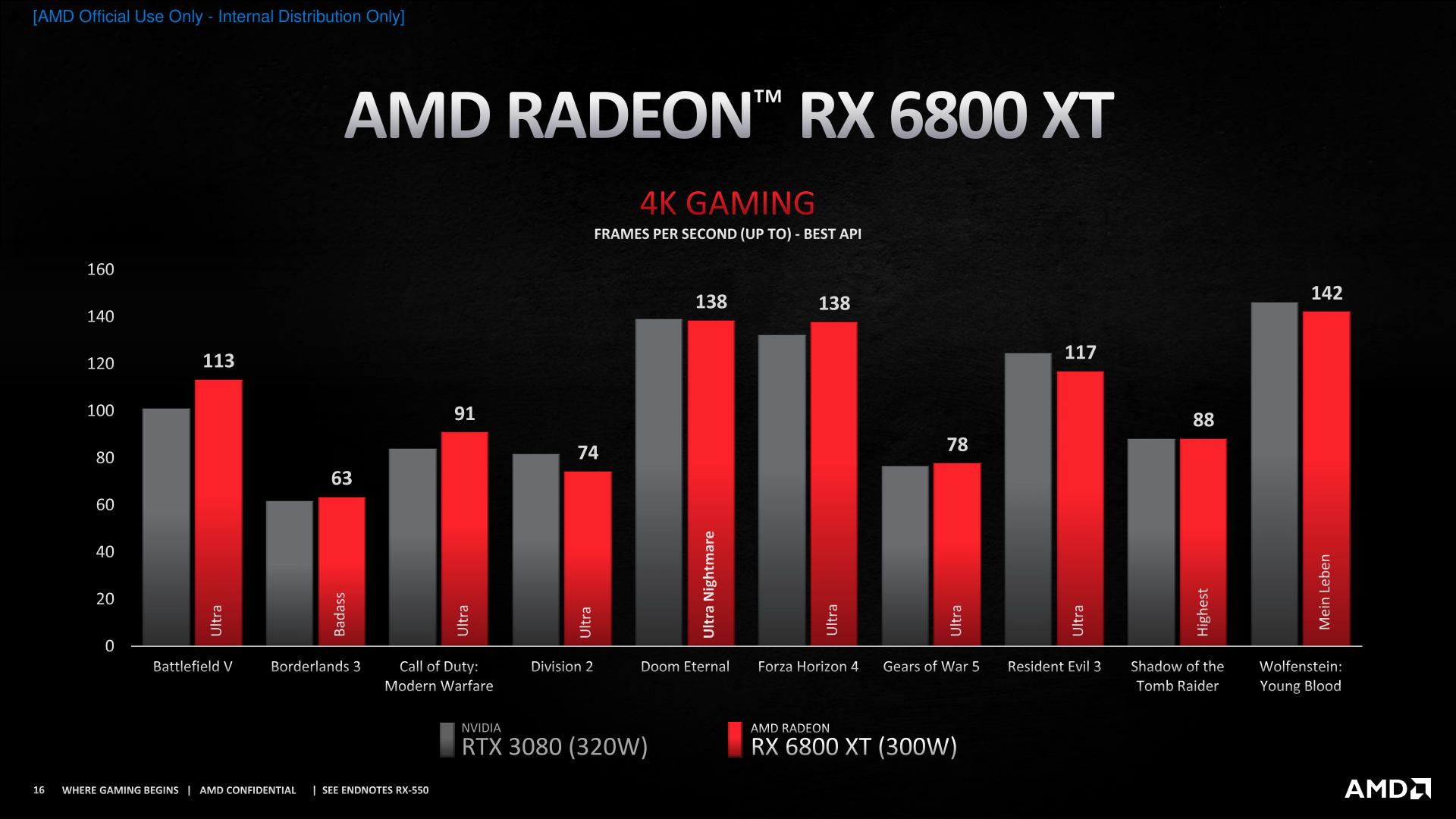
We will of course see for ourselves in the coming weeks just how AMD’s performance stacks up to the rest of the market. But if AMD’s numbers are accurate and representative of the broader ecosystem of graphics-intensive, AAA games, then the RX 6800 XT launch will be a fun one, with both AMD and NVIDIA’s respective cards jostling for position.
Unfortunately, things aren’t nearly apples-to-apples for AMD’s other performance slides, so a lot more salt is needed here. For the RX 6800, for example, AMD has Smart Access Memory enabled for the RX 6800, even though there’s no comparable feature for the GeForce RTX 2080 Ti, nor can it be used on Intel platforms.
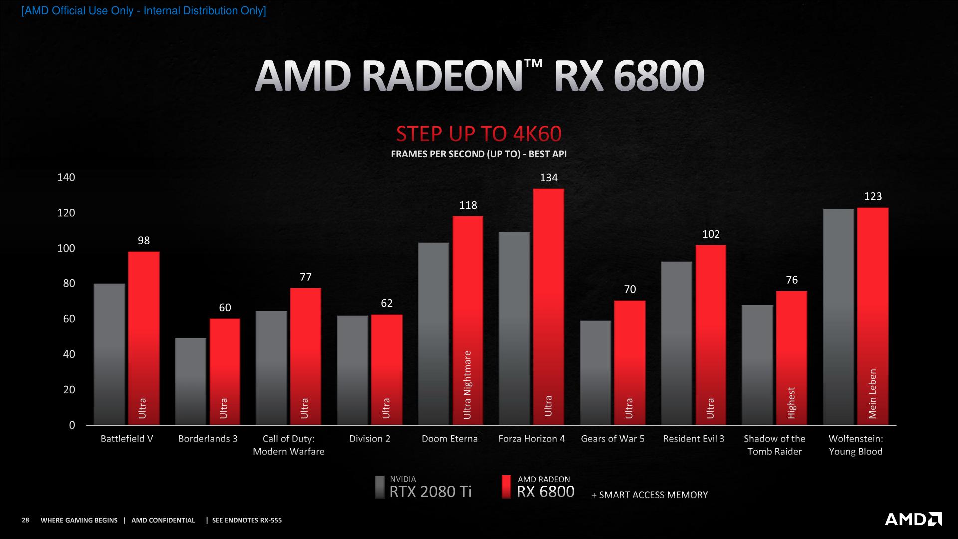

In practice, with a $579 price tag, AMD is already aiming over the RTX 3070. So as long as they can still readily hit that without SAM, then it makes little difference whether it’s included here. But as a matter of practice, we always prefer to see apples-to-apples testing.
Finally, the RX 6900 XT benchmarks are the worst in this regard. Here AMD compares it to an RTX 3090, but with both SAM and their Rage Mode auto-overclocking enabled. So this isn’t even representative of an RX 6900 XT running in its out-of-the-box configuration!
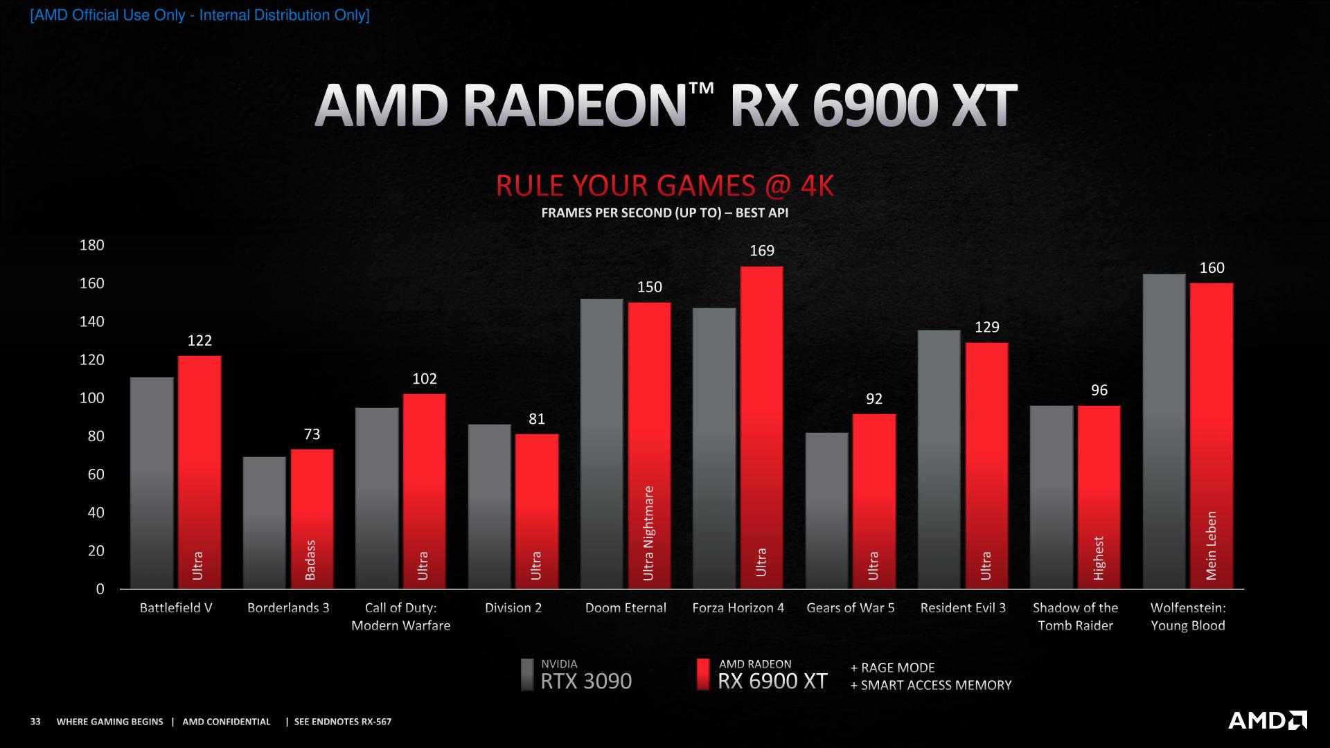
AMD of course want to put its best foot forward here, as these are the cards that will vie for the performance crown and thus bragging rights for this generation of video cards. However it also hints that while AMD will likely get close to the RTX 3090, actually matching NVIDIA’s flagship is likely at the very far edge of what the 6900 XT can do. Without Rage Mode and SAM enabled, the RX 6900 XT would not get quite this close – AMD is seemingly having to wring out every last bit of performance to close the gap.
But like everything else we’ve seen here today, we’ll test this for ourselves in the coming weeks. Ultimately, even if AMD isn’t able to take the crown from NVIDIA, being able to match the RTX 3080 and act as a spoiler the RTX 3090 would be a huge morale boost for AMD’s GPU group.
What’s Next: More RDNA2 GPUs Next Year, RDNA3 Looks At 2022
Wrapping things up with a look at what’s next, AMD’s presentation and briefings also offered a quick glimpse of what’s next for video cards from the company.
First and foremost, AMD isn’t done with RDNA2. The company has confirmed that they’ll be replacing the bulk of their GPU lineup with RDNA2-based parts. Just what “bulk” entails remains to be seen, but I would be surprised to see anything in AMD’s mid-range products, currently occupied by the RDNA (1)-based Navi 10 chips, not to get replaced. Along with greatly improving AMD’s energy efficiency, RDNA2 brings some much-needed features that AMD will want to have to remain competitive with NVIDIA.
Fuzzier is whether we’ll see an RDNA2 GPU to replace Navi 14. AMD’s low-end desktop and mobile-focused GPU would benefit from RDNA2 just as much as AMD’s other segments, but there’s a segment of AMD’s customer base that is extremely cost sensitive, so anything that adds die size (and thus what AMD will charge) could be an issue. For that reason Navi 14 may still kick around for a while, even if it does get an RDNA2 successor.
Overall, I do foresee the RDNA2 GPU stack as being larger than the two (ish) chip stack that RDNA (1) got. Especially with the Infinity Cache and its high area cost, AMD will want to be mindful about die sizes and when they use salvaged chips versus when they make a new, smaller chip entirely. NVIDIA, for reference, used 5 chips for its top-to-bottom Turing family of consumer GPUs in the previous generation.
And of course, this doesn’t even factor in APUs. AMD has stuck with Vega for its APUs, even the most recent Renoir parts. So their APU lineup is ready for a proper refresh, and I expect that we’ll see a lot of RDNA2 used in future APUs, truly cementing RDNA2’s place as a fundamental AMD building block.
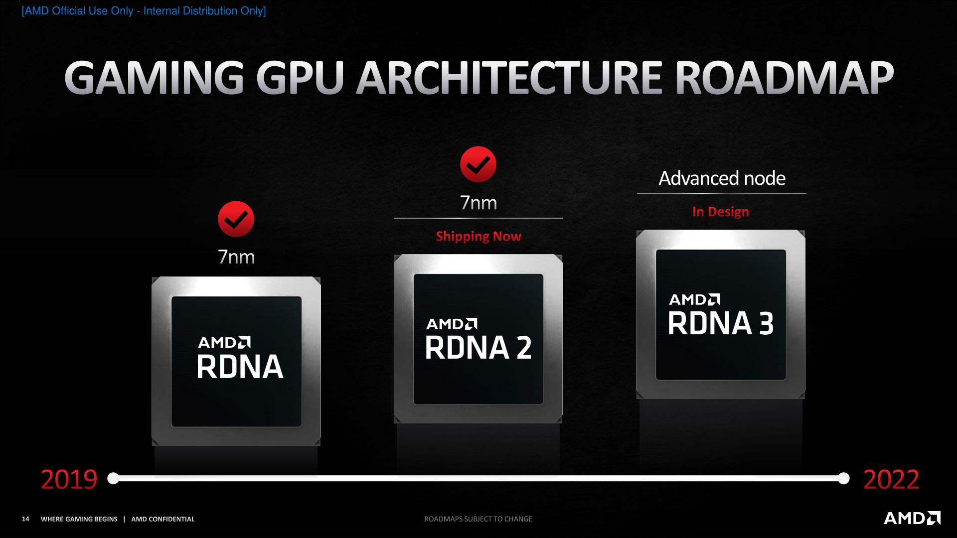
Finally, farther out on the horizon still will be RDNA3. With RDNA2 just now getting ready to ship, RDNA3 is still some time off and AMD is not saying anything further about it. But for today they are reiterating their previously-disclosed GPU roadmap: RDNA3 will be made on an advanced node and will land by the end of 2022, ensuring that AMD never goes too long without something interesting happening in the GPU realm.


274 Comments
View All Comments
The Benjamins - Wednesday, October 28, 2020 - link
The 6800 has 16GB of ram not 14GBSub31 - Wednesday, October 28, 2020 - link
Nowhere in the article does it say 6800 has 14 GB of RAM. It does say that the RAM is 14 Gbps, though, which is correct.Kurosaki - Wednesday, October 28, 2020 - link
16gbpsNikosD - Thursday, October 29, 2020 - link
@RyanAMD could kill 3090 with more TDP of 6900 XT.
What is the real explanation of artificially limiting the full die of 80CUs at low clock speed in order to maintain 300W TDP while you compete with a 350W TDP card like 3090 ?
I mean the excuse of performance per watt increase from 54% of 6800 XT to 65% for 6900 XT compared to RDNA first gen is simply ridiculous.
We are talking here about a flagship card - the 6900 XT - competing with a 350W TDP monster like 3090.
AMD should have gone at least to 355W as some leaks have said before, in order to win clearly the 3090 by a decent margin.
Spunjji - Thursday, October 29, 2020 - link
It's possible the performance just doesn't scale much further with the extra wattage. There must be a reason, as they'd have plenty of time to make the tweak if it were that simple. Maybe the board design just can't support that power?NikosD - Thursday, October 29, 2020 - link
A slightly increase of 72CUs (6800XT) to 80CUs (6900 XT) gave a new card competitive to 3090 using the exact same clocks/TDP (for 6800 XT/6900 XT)So, the architecture scales extremely well.
Also, judging by the rumors and PS5, boost clock could be at least 10% higher.
If they don't want to support a beefier cooler for a reference card, they should allow AIBs to do it.
It is very strange that AMD doesn't allow custom 6900 XT from the beginning.
Could they afraid of a nVidia respond of a 3090 Ti / Titan and they haven't prepared a RDNA2/ HBM2 card or something equivalent ?
The same clock/TDP for 6800 XT and 6900 XT cards, simply doesn't fit.
Spunjji - Thursday, October 29, 2020 - link
10% increase in resources to get a 10% benefit is one thing, but I'm talking about how well the performance scales with additional clock speed vs. power usage. It's possible that throwing another 50W of power at the board will only get them a few percent extra in performance.Designing a card to soak up 300W of power isn't simple, either. Look at the issues Nvidia have had with theirs.
I'd wager they're keeping the 6900XT to themselves because they can't bin enough of the chips to make it worth sending out to AIBs.
This is just me trying to make sense of it, of course - I'm guessing. But it seems more sensible to assume a reason than to assume they'd just... skip the opportunity.
d0x360 - Thursday, October 29, 2020 - link
Well we saw those leaks with a card hitting 2.8ghz.. it's possible they are just holding stuff back for the inevitable 3080ti or supers from nVidia. They could also change to gddr6x, increase the bus size, add memory, add more cache and that alone would probably do the trick but if they also have headroom on the clocks with a TDP increase... It could be huge. AMD with the performance crown for the first time since the 290x.NikosD - Thursday, October 29, 2020 - link
Yes, Ampere looked like it has a frequency wall at 2.0GHz mitigated by a recent driver but I've never expected RDNA2 to have a power wall of 300W as you describe it.All the latest leaks and rumors were talking about custom 3080 cards with more than >350W TDP.
Yes, they could be wrong as in other things regarding RX 6000 series and your guess could be right, but I doubt it.
I mean 300W could be a sweet spot for RDNA2 efficiency, but AMD should/could sacrifice a little or more of its efficiency for a little more performance.
Custom 3080 cards and more tech info about increased TDP behavior of RDNA2 cards will enlighten us in the near future.
Spunjji - Friday, October 30, 2020 - link
I'm not talking about a power *wall*, just a point of rapidly diminishing returns. We've already seen that with Ampere and the 3090 vs the 3080 - the 3090 should be a LOT faster going off specs, but it just isn't. Think of the same way Ryzen CPUs overclock - or, to be precise, don't. They don't draw anywhere near as much power as Intel's best, so in theory there's "headroom", but in reality the design is actually at its limits.AMD have spent the past 8+ years sacrificing efficiency for performance, and when they do so and only get marginal leadership it just gets criticism poured on them (as with the 290X). I don't think pushing for a few percent extra performance at the cost of 50-100W more power makes sense.
As for those leaks about them hitting 2.8Ghz - even if they're true (bearing in mind that there's a cottage industry built around overhyping AMD products and then claiming to be "disappointed"), we have no idea under what circumstances they hit clocks higher than 2.2Ghz and what the resulting performance is.
I'm going with Occam's razor on this: if the architecture could reliably and consistently hit a significantly higher level of performance for about 50W more power, and that would allow them to beat the 3090 in both performance and performance-per-watt, then they'd have done it. But they haven't. Why would they top out with a bleeding-edge bin that *just* misses the target if it were trivial for them not to?