The Card
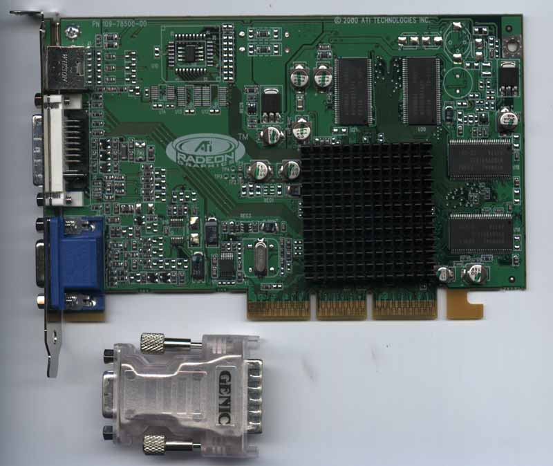
The Radeon VE looks strikingly similar to the Radeon SDR, most likely due to the fact that the two appear to be made on merely the same PCB. In contrast to the faster performing Radeon SDR, as well as other Radeon cards, the Radeon VE comes without a fan, only a heatsink. As we mentioned in our original Radeon DDR review, it seems that any Radeon core running at 183 MHz does not really even need a fan: the fan is most likely only added for aesthetic value, as people associate chips with fans on them as fast. In order to save costs even further, the Radeon VE skips the whole fan and uses just a standard heatsink. The heatsink does get hot to the touch, however it is unlikely that even this heatsink is necessary. It is attached via a layer of thermal glue.
The DVI-I port as well as S-video out port will come standard on every retail Radeon VE card sold. ATI includes these ports so that the user can take advantage of their HydraVision multiple monitor support (more on this later). Also included in every package is a Genic DVI-I to VGA converter that allows the card's DVI port to power any standard 15-pin monitor. Unlike some GeForce2 MX cards that claim TwinView support, users buying the Radeon VE can rest assured that the card will work with nearly every monitor they have, as well as every television with an S-video or composite input port. The DVI-I port is powered by the Radeon VE's internal TMDS transmitter.
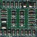
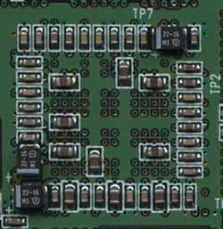
We were speaking about how much space removing both the Charisma engine as well as one of the rendering pipelines saved. By looking at the back of both the Radeon VE as well as the back of the Radeon SDR, we can take a guess (note that the pictures are to scale)..
 |
 |
|
Radeon VE Core
|
Radeon SDR Core
|
The answer seems to be a lot. Estimating die size by the rectangle of transistors on the back of the cards directly behind the core, you can see how much smaller the Radeon VE's core seems to be. This means big money savings for ATI.
Before we go on, let's take a look and see how the Radeon VE's numbers compare to the competition.
|
Video
Card Specification Comparison
|
||||||||
|
ATI
Radeon VE
|
ATI
Radeon SDR
|
NVIDIA
GeForce2 MX
|
Matrox
G450
|
3dfx
Voodoo4 4500
|
||||
| Core |
Rage6C
|
NV11
|
Napalm
(VSA-100)
|
|||||
|
Clock Speed |
183MHz
|
183MHz
|
175MHz
|
125MHz
|
166MHz
|
|||
| Number of Chips |
1
|
1
|
1
|
1
|
1
|
|||
| Rendering Pipelines |
1
|
2
|
2
|
2
|
2
|
|||
| Texels/Clock |
3
|
3
|
2
|
1
|
1
|
|||
| Texels/Second |
549
Million
|
1100
Million
|
700
Million
|
250
Million
|
333
Million
|
|||
| Memory Bus |
64-bit
DDR
|
128-bit
SDR/DDR
|
128-bit
SDR or 64-bit SDR/DDR
|
64-bit
DDR
|
128-bit
SDR
|
|||
| Memory Clock |
183MHz
DDR (366 MHz)
|
183
MHz SDR
|
166MHz
SDR
|
166MHz
DDR
|
166MHz
SDR
|
|||
| Memory Bandwidth |
2.9
GB/s
|
2.9
GB/s
|
2.7
GB/s
|
2.7
GB/s
|
2.7
GB/s
|
|||
| Manufacturing Process |
0.18-micron
|
0.25-micron
(Enhanced)
|
||||||


0 Comments
View All Comments