EUVL
Foundries started limited usage of extreme ultraviolet (EUV) lithography for high-volume manufacturing (HVM) of chips in 2019. At the time, ASML's Twinscan NXE scanners were good enough for production, but the full EUV ecosystem was not quite there. One of the things that impacted EUV was the lack of protective pellicles for photomasks, which limited usage of EUV tools and affected yields. Fortunately, the situation with pellicles has finally improved thanks to the recent introduction of production-ready EUV pellicles, and matters promise to get even better in the coming years. Protecting Precious Reticles ASML has made a great progress with its Twinscan NXE EUV lithography tools in the recent years, improving performance of light source, availability time, and productivity. Its industry peers have also done a...
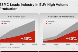
TSMC: We have 50% of All EUV Installations, 60% Wafer Capacity
One of the overriding central messages to TSMC’s Technology Symposium this week is that the company is a world leader in semiconductor manufacturing, especially at the leading edge process...
32 by Dr. Ian Cutress on 8/27/2020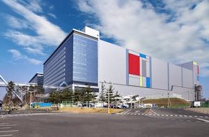
Samsung to Produce DDR5 in 2021 (with EUV)
Samsung is on track to start volume production of DDR5 and LPDDR5 memory next year using a manufacturing technology that will take advantage of extreme ultraviolet lithography (EUVL). In...
20 by Anton Shilov on 3/25/2020
TSMC & Broadcom Develop 1,700 mm2 CoWoS Interposer: 2X Larger Than Reticles
With transistor shrinks slowing and demand for HPC gear growing, as of late there has been an increased interest in chip solutions larger than the reticle size of a...
18 by Anton Shilov on 3/4/2020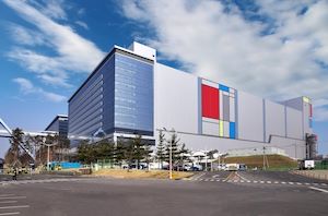
Samsung Starts Mass Production at V1: A Dedicated EUV Fab for 7nm, 6nm, 5nm, 4nm, 3nm Nodes
Samsung Foundry has started mass production of chips using its 6LPP and 7LPP manufacturing processes at its new V1 fab. The new facility employs one of the industry’s first...
30 by Anton Shilov on 2/20/2020
ASML Ramps Up EUV Scanners Production: 35 in 2020, Up to 50 in 2021
ASML shipped 26 extreme ultraviolet lithography (EUVL) step-and-scan systems to its customers last year, and the company plans to increase shipments to around 35 in 2020. And the ramp-up...
22 by Anton Shilov on 1/23/2020
TSMC Boosts CapEx by $1 Billion, Expects N5 Node to Be Major Success
TSMC is on track to begin high-volume production of chips using its 5 nm technology in the coming months, the company said in its conference call last week. While...
40 by Anton Shilov on 1/22/2020
TSMC: 5nm on Track for Q2 2020 HVM, Will Ramp Faster Than 7nm
TSMC’s 5 nm (N5) manufacturing technology is projected to provide significant benefits when it comes to performance, power, and area scaling, which is why the contract maker of semiconductors...
27 by Anton Shilov on 10/23/2019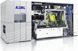
EUV Demand is Up: EUV Device Manufacturer ASML Beats Sales Estimates
Between the smartphone revolution, cloud computing, and the Internet of Things, the demand for cutting-edge chips has never been higher. And if you have any doubts about that, then...
46 by Anton Shilov on 10/16/2019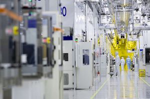
Samsung’s Aggressive EUV Plans: 6nm Production in H2, 5nm & 4nm On Track
Samsung Foundry formally started to produce chips using its 7LPP (7 nm low power plus) fabrication process last October and has not slowdown development of its manufacturing technologies since...
42 by Anton Shilov on 7/31/2019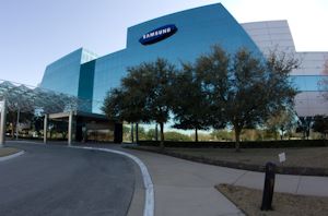
Samsung Completes Development of 5nm EUV Process Technology
Samsung Foundry this week announced that it has completed development of its first-generation 5 nm fabrication process (previously dubbed 5LPE). The manufacturing technology uses extreme ultraviolet lithography (EUVL) and...
21 by Anton Shilov on 4/17/2019
ASML to Ship 30 EUV Scanners in 2019: Faster EUV Tools Coming
ASML said last week that it planned to ship 30 extreme ultraviolet scanners in 2019, up significantly from 2018. The plan is not surprising, as demand for EUV lithography...
17 by Anton Shilov on 1/28/2019
TSMC Kicks Off Volume Production of 7nm Chips
TSMC last week announced that it had started high volume production (HVM) of chips using their first-gen 7 nm (CLN7FF) process technology. The contract maker of semiconductors says it...
63 by Anton Shilov on 4/24/2018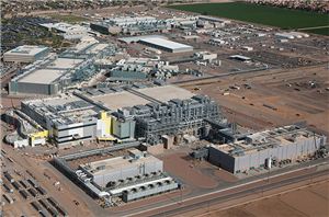
Intel to Equip Fab 42 for 7 nm
Intel this week announced plans to bring its Fab 42 online to produce semiconductors using a 7 nm fabrication process. It will take three to four years, and the...
24 by Anton Shilov on 2/9/2017
EUV Lithography Makes Good Progress, Still Not Ready for Prime Time
At the recent annual SPIE Advanced Lithography conference, Intel, TSMC and other leading semiconductor companies said that significant strides have been made in extreme ultraviolet lithography (EUVL) over the...
38 by Anton Shilov on 3/10/2016


