SoIC

TSMC's 3D-stacked system-on-integrated chips (SoIC) advanced packaging technologies is set to evolve rapidly. In a presentation at the company's recent technology symposium, TSMC outlined a roadmap that will take the technology from a current bump pitch of 9μm all the way down to a 3μm pitch by 2027, stacking together combinations of A16 and N2 dies. TSMC has a number of advanced packaging technologies, including 2.5D CoWoS and 2.5D/3D InFO. Perhaps the most intriguing (and complex) method is their 3D-stacked system-on-integrated chips (SoIC) technology, which is TSMC's implementation of hybrid wafer bonding. Hybrid bonding allows two advanced logic devices to be stacked directly on top of each other, allowing for ultra-dense (and ultra-short) connections between the two chips, and is primarily aimed at high performance...
TSMC to Expand CoWoS Capacity by 60% Yearly Through 2026
Customer demand for AI and HPC processors is driving a much greater use of advanced packaging technologies, particularly TSMC's chip-on-wafer-on-substrate (CoWoS) services. As things stand, TSMC is just barely...
8 by Anton Shilov on 5/21/2024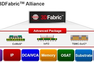
TSMC Opens Advanced Backend Packaging Fab for AI and HPC Products
TSMC on Friday formally opened its Advanced Backend Fab 6 facility, which it will be using to expand the company's capacity for building high-end, multi-chiplet products. The facility is...
1 by Anton Shilov on 6/9/2023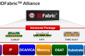
TSMC Forms 3DFabric Alliance to Accelerate Development of 2.5D & 3D Chiplet Products
Currently the majority of high-end processors are monolithic, but design methodologies are slowly but surely shifting to multi-chiplet modules as leading-edge fabrication technologies get more expensive to use. In...
9 by Anton Shilov on 10/27/2022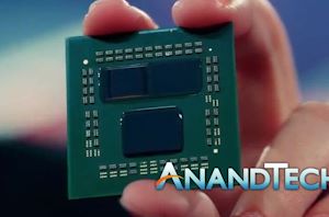
AMD Demonstrates Stacked 3D V-Cache Technology: 192 MB at 2 TB/sec
The AMD team surprised us here. What seemed like a very par-for-the-course Computex keynote turned into an incredible demonstration of what AMD is testing in the lab with TSMC’s...
93 by Dr. Ian Cutress on 5/31/2021
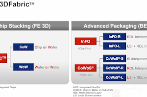
3DFabric: The Home for TSMC’s 2.5D and 3D Stacking Roadmap
Interposers. EMIB. Foveros. Die-to-die stacking. ODI. AIB.TSVs. All these words and acronyms have one overriding feature – they are all involved in how two bits of silicon physically connect...
9 by Dr. Ian Cutress on 9/2/2020


