Intel Architecture Day 2021: Alder Lake, Golden Cove, and Gracemont Detailed
by Dr. Ian Cutress & Andrei Frumusanu on August 19, 2021 9:00 AM ESTConclusions
Alder Lake is set to come to market for both desktop and mobile, and we’re expecting the desktop hardware to start to appear by the end of the year – perhaps a little later for the rest of the family, but all-in-all we expect Intel is experiencing some serious squeaky bum time regarding how all the pieces will fit in place at that launch. The two main critical factors are operating systems and memory.
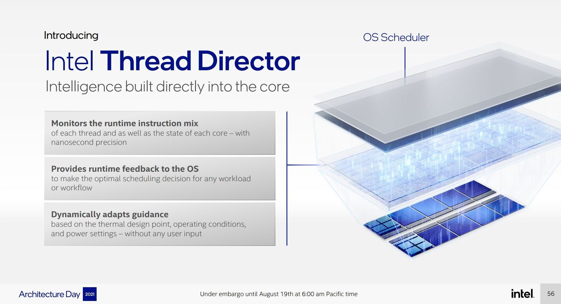
Because Alder Lake is Intel’s first full-stack attempt to commercialize a hybrid design, it has had to work closely with Microsoft to enable all the features it needs to make managing a hybrid core design properly beneficial to users. Intel’s new Thread Director Technology couples an integrated microcontroller per P-core and a new API for Windows 11 such that the scheduler in the operating system can take hints about the workflow on the core at a super fine granularity – every 30 microseconds or so. With information about what each thread is doing (from heavy AVX2 down to spin lock idling), the OS can react when a new thread needs performance, and choose which threads need to be relegated down to the E-core or as a hyperthread (which is classified as slower than an E-core).
When I first learned Alder Lake was going to be a hybrid design, I was perhaps one of the most skeptical users about how it was going to work, especially with some of the limits of Windows 10. At this point today however, with the explanations I have from Intel, I’m more confident than not that they’ve done it right. Some side off-the-record conversations I have had have only bolstered the idea that Microsoft has done everything Intel has asked, and users will need Windows 11 to get that benefit. Windows 10 still has some Hardware Guided Scheduling, but it’s akin to only knowing half the story. The only question is whether Windows 11 will be fully ready by the time Alder Lake comes to market.
For memory, as a core design, Alder Lake will have support for DDR4 and DDR5, however only one can be used at any given time. Systems will have to be designed for one or the other – Intel will state that by offering both, OEMs will have the opportunity to use the right memory at the right time for the right cost, however the push to full DDR5 would simplify the platform a lot more. We’re starting to see DDR5 come to the consumer market, but not in any volume that makes any consumer sense – market research firms expect the market to be 10% DDR5 by the end of 2022, which means that consumers might have to be stay with DDR4 for a while, and vendors will have to choose whether to bundle DDR5 with their systems. Either way, there’s no easy answer to the question ‘what memory should I use with Alder Lake’.
Through The Cores and The Atoms
From a design perspective, both the P-core and E-core are showcasing substantial improvements to their designs compared to previous generations.
The new Golden Cove core has upgraded the front-end decoder, which has been a sticking point for analysis of previous Cove and Lake cores. The exact details of how they operate are still being kept under wraps, but having a 6-wide variable length decoder is going to be an interesting talking point against 8-wide fixed-length decoders in the market and which one is better. The Golden Cove core also has very solid IPC figure gains, Intel saying 19%, although the fact there are some regressions is interesting. Intel did compare Golden Cove to Cypress Cove, the backported desktop core, rather than Willow Cove, the Tiger Lake core, which would have been a more apt comparison given that our testing shows Willow Cove slightly ahead. But still, around 19% is a good figure. Andrei highlights in his analysis that the move from a 10-wide to a 12-wide disaggregated execution back-end should be a good part of that performance, and that most core designs that go down this route end up being good.
However, for Gracemont, Intel has taken that concept to the extreme. Having 17 execution ports allows Intel to clock-gate each port when not in use, and even when you couple that with a smaller 5-wide allocation dispatch and 8-wide retire, it means that without specific code to keep all 17 ports fed, a good number are likely to be disabled, saving power. The performance numbers Intel provided were somewhat insane for Gracemont, suggesting +8% performance over Skylake at peak power, or a variety of 40% ST perf/power or 80% MT perf/power against Skylake. If Gracemont is truly a Skylake-beating architecture, then where have you been! I’m advocating for a 64-core HEDT chip tomorrow.
One harsh criticism Intel is going to get back is dropping AVX-512 for this generation. For the talk we had about ‘no transistor left behind’, Alder Lake dropped it hard. That’s nothing to say if the functionality will come back later, but if rumors are believed and Zen 4 has some AVX-512 support, we might be in a situation where the only latest consumer hardware on the market supporting AVX-512 is from AMD. That would be a turn-up. But AMD’s support is just a rumor, and really if Intel wants to push AVX-512 again, it will have a Sisyphean task to convince everyone it’s what the industry needs.
Where We Go From Here
There are still some unanswered questions as to the Alder Lake design, and stuff that we will test when we get the hardware in hand. Intel has an event planned for the end of October called the Intel InnovatiON event (part of the ON series), which would be the right time to introduce Alder Lake as a product to the world. Exactly when it comes to retail will be a different question, but as long as Intel executes this year on the technology, it should make for an interesting competition with the rest of the market.


223 Comments
View All Comments
name99 - Saturday, August 21, 2021 - link
As always the devil is in the details :-)Basic loop buffers, as in the LSD (introduced one gen before Nehalem, with Core2) have been with us forever, including early ARM chips and the early PA Semi chips, going on to Apple Swift.
But the basic loop buffer can not deal with branches (because part of the system is to switch off branch prediction!). Part of what makes the Apple scheme interesting and exceptional is that it's this graduated scheme that manages to extract much of the energy win from the repetition of loops while being able to cover a much wider variety of loops including those with (not too awful) patterns of function calls and branches.
Comparing details is usually unhelpful because different architectures have different concerns; obviously x86 has decode+variable length concerns which is probably THE prime concern for how their structure their attempts to extract performance and energy savings from loops,
On the Apple side, I would guess that Mapping (specifically detecting dependencies within a Decode group of 8 instructions, ie what register written by instruction A is immediately read by successor instruction B) is a high-energy task, and a future direction for all these loop techniques on the Apple side might be to somehow save these inter-instruction-dependencies in the loop storage structure? This is, obviously, somewhat different from Intel or AMD's prime concern with their loops, given that even now they max out at only 5 (perhaps soon 6) wide in the mapping stage, and don't need to know as much for mapping because they don't do as much zero-cycle work in the stage right after Mapping.
GeoffreyA - Sunday, August 22, 2021 - link
Thanks. I suppose storing the dependancy information would be of use even in non-loop cases, because of the amount of work it takes. Then again, it might add greater complexity, which is always a drawback.mode_13h - Sunday, August 22, 2021 - link
> I would guess that Mapping (specifically detecting ... what register written by> instruction A is immediately read by successor instruction B) is a high-energy task
So, do you foresee some future ISA trying to map these out at compile-time, like Intel's ill-fated EPIC tried to do? On the one hand, it bloats the instruction size with redundant information. On the other, it would save some expensive lookups, at runtime. I guess you could boil it down to a question of whether it takes more energy for those bits to come in from DRAM and traverse the cache hierarchy vs. doing more work inside the core.
The other idea I have is that if the CPU stores some supplemental information in its i-cache, then why not actually flush that out to L3 & DRAM, rather than recompute it each time? The OS would obviously have to provide the CPU with a private data area, sort of like a shadow code segment, but at least the ISA wouldn't have to change.
mode_13h - Saturday, August 21, 2021 - link
Thanks. Very nice incremental explanation of a loop buffer, trace cache, and L0.> n-way set-associative cache means you now have, n slots associated with a given index.
> So if you have 8 slots, you can hold 8 lines with that same index,
> ie 8 addresses with those same middle bits.
> BUT how do you know WHICH of those 8 lines you want?
Yeah, I know how a set-associative cache works. The simplistic explanation is that there's a n-entry CAM (Content-Addressable Memory) which holds the upper bits of the addresses (I think what you're calling Tags) for each cache line in a set. So, a cache lookup involves up to n (I suppose 8, in this case) comparisons against those upper bits, to find out if any of them match the requested address. And, ideally, we want the hardware to do all those comparisons in parallel, so it can give a quicker answer where our data is (or fetch it, if the cache doesn't have it).
Even at that level, cache is something not enough software developers know about. It's really easy to thrash a normal set-associative cache. Just create a 2D array with a width that's a factor or an integral multiple of a cache set size and do a column-traversal. If you're lucky, your entire array fits in L3. If not... :(
> which of these 8 possible lines is of interest is called a WAY.
Where I first learned about CPU caches, they called it a set. So, an 8-way set-associative cache had 8 sets.
> by storing the cache way, you can access a cache with the speed ...
> and energy ... of a direct-mapped cache.
Yup. That's what I thought you were saying. So, the way/set + offset is basically an absolute pointer into the cache. And a bonus is that it only needs as many bits as the cache size, rather than a full address. So, a 64k cache would need only 16 bits to uniquely address any content it holds.
GeoffreyA - Thursday, August 19, 2021 - link
I believe the reservation station is that portion which contains the scheduler and physical register files. In Intel, it's been unified since P6, compared to AMD's split/distributed scheduler design and, I think, Netburst.name99 - Thursday, August 19, 2021 - link
"Intel is noting that they’re doing an increased amount of dependency resolution at the allocation stage, actually eliminating instructions that otherwise would have to actually emitted to the back-end execution resources."Again presumably this means "executing" instructions at Rename (or earlier) rather than as actual execution.
Apple examples are
- handling some aspects of branches (for unconditional branches) at Decode
- zero cycle move. This means you treat a move from one register to another by creating a second reference to the underlying physical register. Sounds obvious, the trick is tracking how many references now exist to a given physical register and when it can be freed. It's tricky enough that Apple have gone through three very different schemes so far.
- zero cycle immediates. The way Apple handle this is a separate pool of ~40 integer registers dedicated to handling MOV xn, # (ie load xn with immediate value #), and the instruction is again handled to Rename.
Intel could do the same.They already do this for zero idioms, of course.
- then there are weirder cases like value prediction where again you insert the value into the target register at Rename. The instruction still has to be validated (hence executed in some form) but the early insertion improves. Apple does this for certain patterns of loads, but the details are too complicated for here.
mode_13h - Friday, August 20, 2021 - link
Thanks again!name99 - Thursday, August 19, 2021 - link
"Someone please remind us what a reservation station is?"After an instruction is decoded it passes through Rename where resources it will need later (like a destination register, or a load/store queue entry) are allocated.
Then it is placed in a Scheduling Queue. It sits in the queue until its dependencies are resolved (ie ADD x0, x1, x2 cannot execute until the values of x1 and x2 are known.
This Scheduling Queue is also called a Reservation Station.
There is a huge dichotomy in design here. Intel insists on using a single such queue, everyone else uses multiple queues. Apple have a queue per execution unit, ala https://twitter.com/dougallj/status/13739734787312... (this is not 100% correct, but good enough).
The problem with a large queue is meeting cycle time. The problem with multiple queues is that they can get unbalanced. It's sad if you are executing integer only code and can't use the FP queue slots. Even worse is if you have one of your integer queues totally full, and the others empty, so only that one queue dispatches work per cycle.
Apple solve these in a bunch of ways.
First note the Dispatch Buffer in front of the Queues. This accepts instructions up to 8-wide per cycle from Rename, and sends as many as possible to the Scheduling Queues. It engages in load balancing to make sure that queues are always as close to evenly filled as possible.
Secondly the most recent Apple designs pair the Scheduling Queues so that, ideally, each queue issues one instruction, but if a Queue cannot find a runnable instruction, it will accept the second choice runnable candidate from its paired queue.
Queues and scheduling are actually immensely complicated. You have hundreds of instructions, all of which could depend in principle on any earlier instruction, so how do track (at minimal area and energy) all these dependencies? Apple appears to use a Matrix Scheduler with a TRULY ASTONISHINGLY CLEVER dependency scheme. A lot about the M1 impresses me, but if I had to choose one thing it might be this.
It's way too complicated to describe here, but among the things you need to bear in mind are
- you want to track which instructions depend on which
- you want to track the age of instructions (so that when multiple instructions are runnable, earliest go first)
- you need to handle Replay. I won't describe this here, but for people who know what it is, Apple provide
+ cycle-accurate Replay (no randomly retrying every four cycles till you finally succeed!) AND, most amazingly
+ perfect DEMAND Replay (only the instructions, down a chain of dependencies) that depended on a Replay are in turn Replayed (and, again, at the cycle accurate time)
+ if you think that's not amazing enough, think about what this implies for value prediction, and how much more aggressive you can be if the cost of a mispredict is merely a cycle-accurate on-demand Replay rather than a Flush!!!
mode_13h - Friday, August 20, 2021 - link
Wow, you're on a roll!name99 - Thursday, August 19, 2021 - link
"> full-line-write predictive bandwidth optimisation ... where the core can greatly improve> bandwidth by avoiding RFO reads of cache lines that are going to be fully rewritten"
Of course this is one of those "about time" optimizations :-)
Apple (it's SO MUCH EASIER with a decent memory model, so I am sure also ARM) have had this for years of course. But improvements to it include
- treat all-zero lines as special cases that are tagged in L2/SLC but don't require transferring data on the NoC. Intel had something like this in IceLake that, after some time, they switched off with microcode update.
- store aggregation is obvious and easy if your memory model allows it. But Apple also engages in load aggregation (up to a cache line width) for uncachable data. I'm not sure what the use cases of this are (what's still uncachable in a modern design? reads rather than DMA from PCIe?) but apparently uncachable loads and stores remain a live issue; Apple is still generating patents about them even now.
- Apple caches all have a bit per line that indicates whether this line should be treated as streaming vs LRU. Obviously any design that provides non-temporal loads/stores needs something like that, but the Apple scheme also allows you to mark pages (or range registers, which are basically BATs -- yes PPC BATs are back, baby!) as LRU or streaming, then the system will just do the right thing whether that data is accessed by load/stores, prefetch or whatever else.
BTW, just as an aside, Apple's prefetchers start at the load-store unit, not the L1. Meaning they see the VIRTUAL address stream.) This in turn means they can cross page boundaries (and prefetch TLB entries for those boundary crossings). They're also co-ordinated so that each L1 is puppeting what it want the L2 prefetcher to do for it, rather than having L1 and L2 prefetchers working independently and hoping that it kinda sorta results in what you want. And yes, of course, tracking prefetching efficiency and throttling when appropriate have always been there.