SK Hynix Adds HBM2 to Catalog: 4 GB Stacks Set to Be Available in Q3
by Anton Shilov on August 1, 2016 10:00 AM EST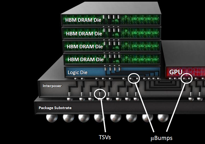
SK Hynix has quietly added its HBM Gen 2 memory stacks to its public product catalog earlier this month, which means that the start of mass production should be imminent. The company will first offer two types of new memory modules with the same capacity, but different transfer-rates, targeting graphics cards, HPC accelerators and other applications. Over time, the HBM2 family will get broader.
SK Hynix intends to initially offer its clients 4 GB HBM2 4Hi stack KGSDs (known good stack dies) based on 8 Gb DRAM devices. The memory devices will feature a 1024-bit bus as well as 1.6 GT/s (H5VR32ESM4H-12C) and 2.0 GT/s (H5VR32ESM4H-20C) data-rates, thus offering 204 GB/s and 256 GB/s peak bandwidth per stack. Earlier this year a representative for SK Hynix revealed plans (in an interview with Golem.de) to start volume production of 4 GB HBM2 KGSDs in Q3 and the addition of the devices into product catalog confirms this information. Keep in mind that memory companies usually make announcements about the start of mass production when they are ready to deliver the first batch of new DRAM to a customer(s). Therefore, it is possible that SK Hynix may already be producing HBM2 stacks.
| Specifications of SK Hynix's HBM2 Memory Chips | ||||||||
| Part Number | Density | Data Rate | Bandwidth per Stack |
Packaging | Feature | Availability | ||
| H5VR32ESM4H-20C | 4 GB | 2.0 GT/s | 256 GB/s | 5mKGSD | 4Hi stack, VDD/VDDQ=1.2V | Q3'16 | ||
| H5VR32ESM4H-12C | 1.6 GT/s | 204 GB/s | ||||||
As outlined in our article published earlier this year, HBM2 memory can stack two, four or eight DRAM devices (2Hi, 4Hi, 8Hi stacks) interconnected using through silicon vias (TSVs) on a base logic die per KGSD (known good stacked die). Each DRAM device features two 128-bit channels, which use DDR signaling with a 2n prefetch architecture (256 bits per memory read and write access) and can operate at their own frequency or even in their own mode. SK Hynix uses 21 nm process technology to make its HBM2 memory and eventually plans to offer 2 GB and 8 GB KGSDs (featuring two or eight 8 Gb DRAM ICs) in addition to 4 GB stacks, aimed at providing memory for various applications. All HBM2 memory products from the company will have 1.2 V VDD/VDDQ and will come in new packages featuring 7.75 mm × 11.87 mm (91.99 mm2) dimensions.
Samsung Electronics began to mass produce its 4 GB 4Hi stack HBM2 KGSDs featuring 2 GT/s data-rate earlier this year and NVIDIA employed the new chips for its GP100 GPU. The first NVIDIA-branded card to use the HBM2 is the Tesla P100 compute accelerator, which has 16 GB of HBM2 memory with 720 GB/s bandwidth (as the DRAM interface operates at about 1.4 GT/s data-rate).

Speaking of HBM2 usage by commercial SoCs, last year SK Hynix said that it worked with 10 companies on various projects (including ASICs, x86 processors, ASSPs and FPGAs) featuring HBM memory (both generations), which indicates that the interest for multi-layer high-bandwidth DRAM is here. However, so far only AMD and NVIDIA have introduced actual products featuring HBM and HBM2.
When it comes to the original HBM, it is worth to mention that SK Hynix has removed such stacks from its catalog. It is unknown whether the company continues to ship them to interested parties, but given the fact that there are not a lot of products that utilize HBM1 today, small scale shipments should not be a problem (at least, until SK Hynix phases out its 29 nm production lines). Meanwhile, since HBM2 is here, it is feasible to assume that we are not going to see many new devices utilizing HBM1.
Source: SK Hynix


43 Comments
View All Comments
Mr.AMD - Monday, August 1, 2016 - link
Truly good news, for AMD Vega....tsk2k - Monday, August 1, 2016 - link
Still not coming before 2017ImSpartacus - Monday, August 1, 2016 - link
You're probably right. We could see little Vega in late 2016, but I doubt we'd see both Vegas until 2017nandnandnand - Monday, August 1, 2016 - link
Who is arguing that Vega is coming in 2016? Polaris and Vega in the same year would be dumb.ddriver - Monday, August 1, 2016 - link
Releasing midrange and highend in the same year would be dumb? That's pretty dumb ;)bigboxes - Tuesday, August 2, 2016 - link
Can we just stop with the pissing matches?ImSpartacus - Monday, August 1, 2016 - link
Just like gp102, gp104 and gp106 dropping in the same six month period? Hell, there's still time for gp107 for a clean sweep.3ogdy - Monday, August 1, 2016 - link
Well, yeah that would be dumb. Especially considering they're not addressing the same markets, price-points and customers. Did I mention the all-new and shiny RX-480 gets beaten by 2013's 3.5GB GTX 970? AMD? Until Zen shows up, it feels like YawnMD.Qasar - Monday, August 1, 2016 - link
according to anands own bench:http://www.anandtech.com/bench/product/1748?vs=174...
i wouldn't really call that a beating.. they trade beats back and forth, and anandtech puts 480 (8 gigs of ram )over all better then 970, byt the 4 gig version.. is slower so then you would be correct... but not compared to the 8 gig version of rx480...
RussianSensation - Monday, August 1, 2016 - link
970 loses to the RX 480. https://www.youtube.com/watch?v=-h6GiFqPYN8Once DX12/Vulkan games are added, and future games that will use > 3.5GB of VRAM, RX 480 4-8GB is a far superior graphics card to the 970.
But the part that's flawed in your entire analysis is that RX 480 is the R9 380 successor and RX 490 will be R9 390/390X successor. Therefore, your comparison of RX 480 to 970 is comparing GPus from entirely different classes. Seem you have been reading too much [H]. RX 480 is a GTX1060 competitor and since 1070 replaced 970, AMD hasn't released the 1070's competitor yet (that should be the RX 490).