Western Digital to Use RISC-V for Controllers, Processors, Purpose-Built Platforms
by Anton Shilov on December 14, 2017 5:00 PM EST- Posted in
- Storage
- CPUs
- Arm
- Western Digital
- SanDisk
- RISC-V
- Esperanto Technologies
Western Digital recently announced plans to use the RISC-V ISA across its existing product stack as well as for future products that will combine processing and storage. The company plans to develop RISC-V cores internally and license them from third parties to use in its own controllers and SoCs, along with using third-party RISC-V based controllers. To develop the RISC-V ecosystem, Western Digital has already engaged in partnerships and investments in various companies working on RISC-V projects. For example, recently Western Digital invested in Esperanto Technologies, a company led by experienced CPU designers.
Given the diverse portfolio of products that Western Digital has today as well as its longer-term intention to move compute closer to data (by embracing in-storage computing, for example), it is evident that Western Digital is going to need a diverse portfolio of compute cores with significantly different performance and feature set. In fact, Western Digital will need two groups of cores, one for storage devices, and another for processing data. Western Digital says that it does not want to develop all the silicon it needs in house, but it will likely have to increase its chip investments in the future.
“We intend to develop some processor cores internally, we also expect to use many other companies’ processor cores to complement our own and are currently evaluating several technologies,” a statement by Western Digital reads.
Since the RISC-V ecosystem is early stages of development, the transition to new cores is not going to happen overnight, but will likely be slow, gradual and will span for many years, if not decades. The first products from Western Digital with RISC-V cores will ship in late 2019, or early 2020, says Western Digital without going into details.
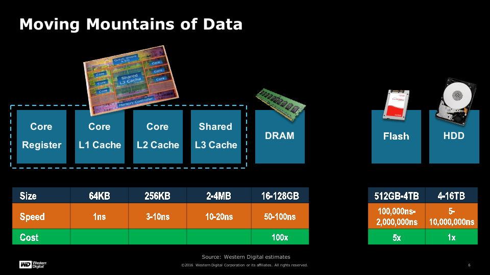
ZetaBytes and PetaFLOPS
As the world generates more data, new storage devices need to store zetabytes of information. HDDs and SSDs have been evolving rather rapidly in the recent years, but their evolution requires not only relentlessly increasing areal density for magnetic media and higher bit density for NAND flash (or other types of memory), but also more processing horsepower. Modern HDD and SSD use controllers that contain multiple processing cores for management, signal processing, contemporary ECC algorithms and other operations.
For example, for today’s TLC/3D TLC NAND memory, SSD controllers already use LDPC with 120bits/1KB recovery in order to correct read errors that occur with the latest types of NAND and thus maximize endurance rating of modern flash memory. Going forward, SSD controllers will need to use stronger algorithms as the industry moves to higher bit densities with TLC and then QLC architectures. As a result, SSD controllers will have to use better cores with higher performance.
Hard drives for their part do not require as vast compute resources as SSDs do, but their processing requirements are also growing because of new magnetic recording technologies, increasing areal densities and more sophisticated functionality (e.g., NAND flash-based caching, health management, QoS enhancements, etc.). Western Digital says that its current products consume about a billion of compute cores per year and the consumption is rising. Given the current SSD/HDD trends, going forward Western Digital is going to consume more cores in general and at least some of those cores will have to be more powerful than the ones the company uses today. Considering the fact that at present there are almost no commercial products based on RISC-V, Western Digital’s plan essentially involves bringing development of a substantial amount of SoCs, controllers, microcontrollers and other chips in-house (more on this later).

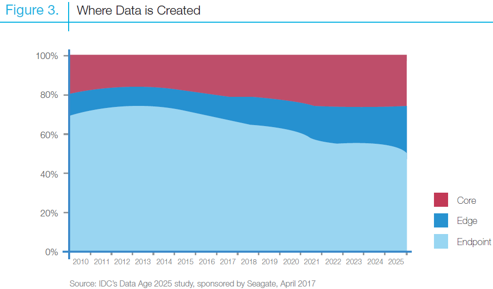
Earlier this year IDC and Seagate published a paper, which claims that 16.1 ZB (ZetaBytes) of data was generated worldwide in 2016 and predicts that the global datasphere would grow by an order of magnitude to 163 ZB by 2025. If the prediction turns out to be correct, demand for high-end storage products by Western Digital, Seagate, Samsung, Micron, Toshiba and others will only grow going forward. This is an important factor for existing business of these companies, but there is another aspect that is not discussed often.
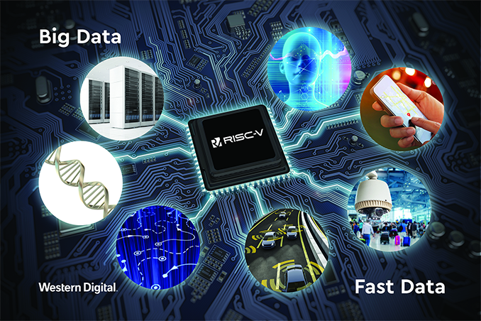
The amount of data that requires real-time processing and low latency is growing and there are cases when Endpoint devices (smartphones, cameras, wearables, cars, PCs, etc.) cannot process it locally, which is why the data has to be sent to more powerful computers. Since processing has to be done as soon as possible, the data is sent to the nearest servers featuring appropriate horsepower. Such machines belong to the Edge category and include server rooms, servers in the field, and smaller datacenters located regionally (as IDC puts it). Since the amounts of generated data is going to grow, Edge servers and Core servers (located in large datacenters) will naturally require more compute horsepower. In the end, the more ZetaBytes stored, the more PetaFLOPS (or even ExaFLOPS) needed to process it.
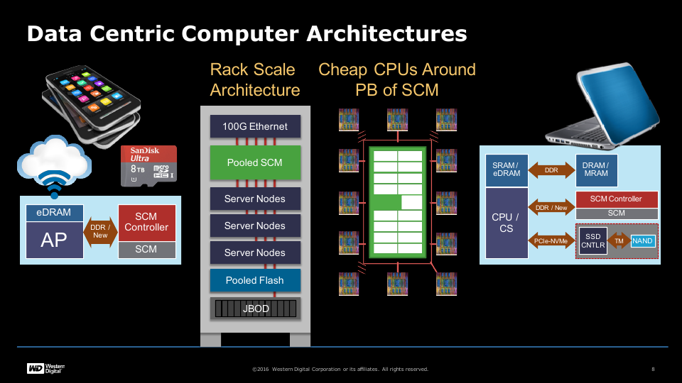
Meanwhile, Western Digital believes that traditional server architectures will not be efficient for Big Data and Fast Data applications in the future. The company believes that processing has to be brought closer to data to minimize data movement at the Edge and within Core datacentres. Apparently, this is where Western Digital sees an opportunity for solutions that not only store data, but also process it. This is actually the second part of Western Digital’s plans concerning the RISC-V architecture: use processing cores (and SoCs) that are powerful enough for Big Data and Fast Data processing.
Western Digital Accelerates Chip Development Efforts
As mentioned above, Western Digital nowadays uses a variety of controllers for its HDDs, SSDs, NAS, DAS and various storage platforms tailored for particular needs (such as HGST’s Active Archive System and SanDisk’s/Fusion-io’s InfiniFlash). Over the years, Western Digital and SanDisk have acquired numerous developers of enterprise-class SSDs and flash storage solutions that developed their own controllers and other hardware. By now, all of these assets have been integrated into various product families, some have been discontinued. Meanwhile, all controllers for Western Digital’s products (it does not matter where they were developed) use compute cores based on ARM, ARC and MIPS architectures.
At present, there are no proven RISC-V-based controllers for storage devices, so transitioning to the architecture essentially means that Western Digital will have to develop some controllers itself and encourage other designers to use RISC-V cores. Western Digital confirms that it plans to develop some of the RISC-V cores itself and license other cores from third parties. It is unknown whether companies like Marvell (which supplies select controllers to Western Digital) has any plans concerning RISC-V, but it is safe to say that Western Digital expects at least some of controller developers to adopt the architecture. In fact, the company is eager to help other companies to start using RISC-V for relevant projects.
“We are committing to help lead the advancement of and transition to data-centric, open compute architectures through the work of the RISC-V Foundation,” said Western Digital in a statement. “[We are] committed to advancing RISC-V and is engaged in active partnerships and investments in RISC-V ecosystem partners.”
As Western Digital will transit to controllers featuring RISC-V cores, it will gradually reduce and eventually cease purchasing third-party controllers based on different architectures. For developers of controllers as well as CPU architecture licensees (Arm, Tallwood MIPS, and Synopsys) this means lost revenues. For Western Digital, it means lower royalty payments, increased development costs, and ability to differentiate its storage products from those using off-the-shelf controllers. It does not seem that Western Digital wants to move development of all controllers it uses in-house, but some of the things it buys from others today will have to be developed internally tomorrow. In fact, further vertical integration of Western Digital is unavoidable as the company moves beyond NAND flash in the coming years. We do know that the company has big plans for ReRAM storage class memory and at least initially controllers for SCM-based storage solutions will have to be developed in-house.
It is interesting to note that apart from HDD/SSD controllers, Western Digital uses Intel’s x86 CPUs for NAS and some other devices. Such chips offer significant performance, so replacing them is impossible and this is why WD will continue working with Intel. Nonetheless, it looks like the storage company expects RISC-V-based SoCs to catch up with its NAS requirements in the future.
“As we transform from a data storage company to a data technology company, in general, we expect to continue our existing, highly valued partnerships, while building new relationships with companies and organizations that share a vision for enabling the data-centric world,” said Western Digital.
Moving Computing Closer to Data
Besides using RISC-V-based compute cores for SSD, HDD, NAS, DAS and other controllers, the company plans to advance “RISC-V technology for use in mission-critical applications so that it can be deployed in its products”. In particular, Western Digital wants to create purpose-built architectures for tomorrow’s workloads of Big Data and Fast Data applications. Here is how Western Digital describes data-centric compute architectures that it plans to develop, or at least help develop:
“Data-centric compute architectures will need the ability to scale resources independent of one another,” explained Western Digital. “The architectures for tomorrow will need to enable purpose-built solutions with data-optimized levels of OS processing, specialty processing, memory, storage and interconnect. The extreme data and compute workloads for analytics, machine learning, artificial intelligence and smart systems demand purpose-built architectures.”
It is noteworthy that throughout its RISC-V-related press release, the company avoided using the term “in storage computing”. There are dozens of companies experimenting with ISC and early results look quite promising: offloading select tasks from CPU to SSDs can reduce latencies by a factor of 2-3 while also decreasing power consumption. The key purpose of ISC is to reduce (or even avoid) "expensive" data transfers from a storage device to a processor by performing computing operations on the former. Latency reductions will be crucial in the looming 5G era, especially for edge computing environments.
Western Digital yet has to share details concerning its RISC-V-related ISC projects, but the company did reveal its common vision of data centric compute architectures back at FMS 2016 (albeit, with some bias towards SCM, which is okay because SCM is a good fit for ISC). In general, the company seems to bet on small/inexpensive purpose-built CPU cores, but their actual performance or capabilities are not disclosed at the moment.
Meanwhile, since no actual roadmap has been shown, it does not make a lot of sense to speculate what exactly the company plans to do and when.
Strategic Investment in Esperanto Technologies
Besides announcing its RISC-V plans, Western Digital also disclosed that it had made a strategic investment in Esperanto Technologies, a developer of RISC-V-based SoCs. The company was founded by Dave Ditzel, who co-founded Transmeta in the 1995 and more recently worked at Intel developing HPC products. A strategic investment is a recognition of Esperanto’s potential, but it does not automatically mean that Western Digital intends to use cores developed by this company.
In the meantime, Esperanto’s ongoing projects demonstrate the potential of the RISC-V ISA in general. So far, Esperanto has developed the ET-Maxion core with maximized single-thread performance as well as the ET-Minion energy-efficient core with a vector FPU. These cores will be used for an upcoming 7 nm SoC for AI and machine learning workloads. In adddition, these are the cores that Esperanto will license to other companies.
| Esperanto's Upcoming AI-Focused SoC | |||
| High-Performance Cores | 16 “ET-Maxion” 64-bit RISC-V cores for highest single thread performance | ||
| Energy-Efficient Cores | 4096 “ET-Minion” energy-efficient RISC-V cores with vector FPUs | ||
| Lithography | 7 nm | ||
Long Road Ahead
Western Digital has supported the RISC-V Foundation for years and therefore it understands how well can it scale for its short-term and long-term needs. The disclosure that it had officially become an adopter of the RISC-V architecture probably means that it already has a roadmap concerning cores, controllers and, perhaps, even products on their base. Meanwhile, the transition is going to take quite a while as Western Digital claims that when it is completed, it expects to be shipping two billion RISC-V cores annually. The number of cores to be consumed indicates a significant growth of product unit shipments that does not happen overnight.
Related Reading:
- Western Digital Stuns Storage Industry with MAMR Breakthrough for Next-Gen HDDs
- Western Digital Now Shipping 14 TB HDDs: HGST Ultrastar Hs14 with 1000 Gb/in2
- Western Digital Ships 12 TB WD Gold HDD: 8 Platters and Helium
Sources: Western Digital, Esperanto Technologies, IDC/Seagate


10 Comments
View All Comments
jimjamjamie - Friday, December 15, 2017 - link
Pretty neat, what are the benefits of using RISC-V over ARM?mode_13h - Friday, December 15, 2017 - link
No royalties, primarily. This cannot be understated, when you're talking about shipping billions of cores/year.Also, less legacy.
andychow - Friday, December 15, 2017 - link
RISC-V can support 128-bit (64 object ID + 64 offset) computing, which allows unique identifiers that can allows persistent pointers on a global scale. It may seem excessive, but the world is currently building 4-5 exascale computers, which will require this type of architecture.With RISC-V, the address space is unique over time and space. Any computer supporting this address space is addressable by the name server. I.E you can have domain wide address space.
64-bit isn't enough for global exascale computing. With the strategy WD is adopting, it will be right there and supporting the technology on day one.
peevee - Monday, December 18, 2017 - link
The value of that is really dubious.64-bit address space with byte addressing IS more than enough for any computer, including "exascale" ones (whatever you mean by that - sounds like a meaningless marketing term). And networks will be IPv6 anyway.
RISC-V is a very dull otherwise, no innovation over the myriad existing RISC instruction sets. Basically, it does not solve a single problem which current instruction sets have, preventing the future development of computing.
mode_13h - Tuesday, December 19, 2017 - link
Agreed. I hadn't heard about this feature of RISC-V. But, even if it's as you describe, network communication of any kind (even PCIe) is sufficiently high-latency that you don't need ISA-level support for inter-machine addressing. In cases where an object might reside outside of local memory, it's no big deal for software to explicitly keep a 64-bit pointer + some other 64-bit identifier.The main problem RISC-V solves is no royalties or IP control issues. And that's enough for many (such as WDC). If all it does is break the ARM hegemony over smartphones and much of the embedded space, then it'll be enough. Then, maybe RISC-VI (or an unrelated, open ISA) can be more ambitious and forward-looking.
lada - Tuesday, December 19, 2017 - link
Open ISA, modular (32,64,128 bits). Governed by an independent foundation, to last 50 years. No ISA license.Very efficient instruction encoding tailored for low complexity decoders (small cores, low power big cores).
Base I integer instruction set has ~50 instructions that can boot Linux, lower power than x86 and ARM. Optional modular extensions - Multiply/add, Floating point etc., vector unit (crypto, SIMD floating point unit).Compressed instructions - most used instructions and register combinations take 16 bits instead of 32.
Scalable(small to big cores) and extendable (new instructions, accelerators).
From tiny microcontrollers to Linux capable multicores.
Simple yet with comparable or higher performance on a given manufacturing node than ARM, let alone x86 (have to wait for OOO cores).
Open - no unverifiable NSA blobs :-), what you compile is what you get.
No legacy baggage. Security by ability to audit cores.
Synthesizable (meaning compiling into your SoC or FPGA project).
RV64GC (64 bit instr. set with integer, multiply, float and compressed extension) for off the-shelf shrink-wrapped software like Linux distros and apps.
Your first RISC-V silicon will probably be a future nVidia chip or a WD disk :-D
Regarding 128 bit support, multiple nodes mapped in memory is the goal, to shave off latency by going through network adapter APIs of any kind. To be orthogonal (node+local address), the address must be divided into node part and local part as in internet protocol, which is btw also 128bit (IPV6). Hence 64+64 bits.
Non standard extensions like reduced register versions are available and being standardized.
RISC-V will do the same Linux did for smartphones, home appliances, router, supercomputers etc.
mode_13h - Tuesday, December 19, 2017 - link
> Your first RISC-V silicon will probably be a future nVidia chipThis is a bit misleading. They're only using it for an embedded microcontroller - not the actual compute cores.
Also, I've read there are already issues with the number of incompatible extensions that've been added to the ISA. They really need some sort of namespace scheme for the extensions, and then a chip-specific mapping to pack the opcode space.
lada - Wednesday, December 20, 2017 - link
Extensions are for accelerators, i.e. a special data crunching. basic extensions (it's modular) ale named by a single character (I - integer, M-multiply/add, F- float, D-double precision, A - atomics, V-vector, G=all of IMAFD,C - compressed) and vendor specific BUT standardized start with Z or X alphabet. Ie. Zxxxxx is something developed by some company for machine learning. All extensions are voluntary, it's a way to handle computation to more efficient instructions. Why not.
The base I integer ISA is to be frozen. It's also sufficient for Linux to boot up. Optional basic extensions are here to allow higher performance cores. Small cores, like those embedded in nVidia or WD controller only get extensions they really need.
For general software like Linux distributions and applications (and not to segment the market) the RV64GC is considered a base standard. Therefore the desktop level software can assume that all of the instructions in the RV64IMAFDC(=RV64GC) standard are there.
This modularity allows only subsets of the instructions to be in a cpu for closed designs, and all of the REQUIRED instructions for desktop or server-like cpus. Some companies or university projects add only some instructions from some extensions, for example only multiply instruction, but not all register bit widths combinations. And it's fine, because it's their specific design.
The instruction encoding is well crafted to allow the base instructions to be always in "the same place", in other words, to have always the same instruction format. You can run a program compiled for RV64I standard on any CPU up, because this is the base minimum for all design (embedded and up).
The most expensive part of any CPU are the compilers from various languages. So to allow the 50 years longevity, the encoding of the instructions and register layout has to be frozen.
RISC-V allows instruction encoding - variable length instructions - in multiples of 16 bits. The instruction decoder immediately knows how long the instruction is and can therefore decode other instructions in parallel. x86 has extremely fragmented ISA encoding (thus spending 2/3 of power on just decoding) and ARM or MIPS has fixed 32bit encoding.
Feature seen only on ARM is compressed instructions. Most used ones on RISC-V C extension are packed from 32bits to 16bits and this saves about 25% of code size (useful on small microcontrollers as well as on very complex cores because of smaller cache load). The cpu executes both 32 and 16bit variants, you know. It's 1:1 encoding thus simple to decode.
Whole ISA from 32bit to 128bit fits on a single sheet of paper. On x86 instruction manual is about 5000 pages long and on ARM it's around 5700. For RISC-V it's about 70. Not counting platform specific implementation features - interrupt controller etc. Just the ISA.
And other ecosystem is coming, for example cache coherent protocol in a reference implementation in a Rocket chip and it's off-the chip variant now developed by SiFive.
Last - note that different bit widths of the ISA, i.e. RV32, RV64 and RV128 are different ISAs that assume different register widths. So code for RV32 would not probably run on RV64 machine. Definitely not the other way.
There are 32 integer registers, optionally 32 floating point registers and optionally 32 vector lanes with 4 elements (not 100% sure). There is an extension for only 16 register version, for tiny microcontrollers. Some people from big compute have also raised legitimate questions for standardizing 16 register extension, because the register sets are comparatively big part of the core compared to the other logic ;-) For hundreds of threads on one chip, it really counts.
mode_13h - Thursday, December 21, 2017 - link
> x86 has extremely fragmented ISA encoding (thus spending 2/3 of power on just decoding)This has got to be some kind of worst-case scenario. For one thing, x86 CPUs cache their decoded instructions. And even if they didn't, there's no way decoding uses 2x the power of something like AVX2.
Threska - Tuesday, December 19, 2017 - link
Wonder how well it would fit in with the move to Infinity Fabric (and the Intel equivalent)?