Flash Memory Summit 2018, SK Hynix Keynote Live Blog: NAND Development
by Ian Cutress & Billy Tallis on August 7, 2018 5:21 PM EST
05:23PM EDT - Three parts to this talk
05:23PM EDT - They're going way too fast already
05:23PM EDT - Bits per wafer has increased 60x over the past 10 years
05:23PM EDT - Increasing NAND density in the future
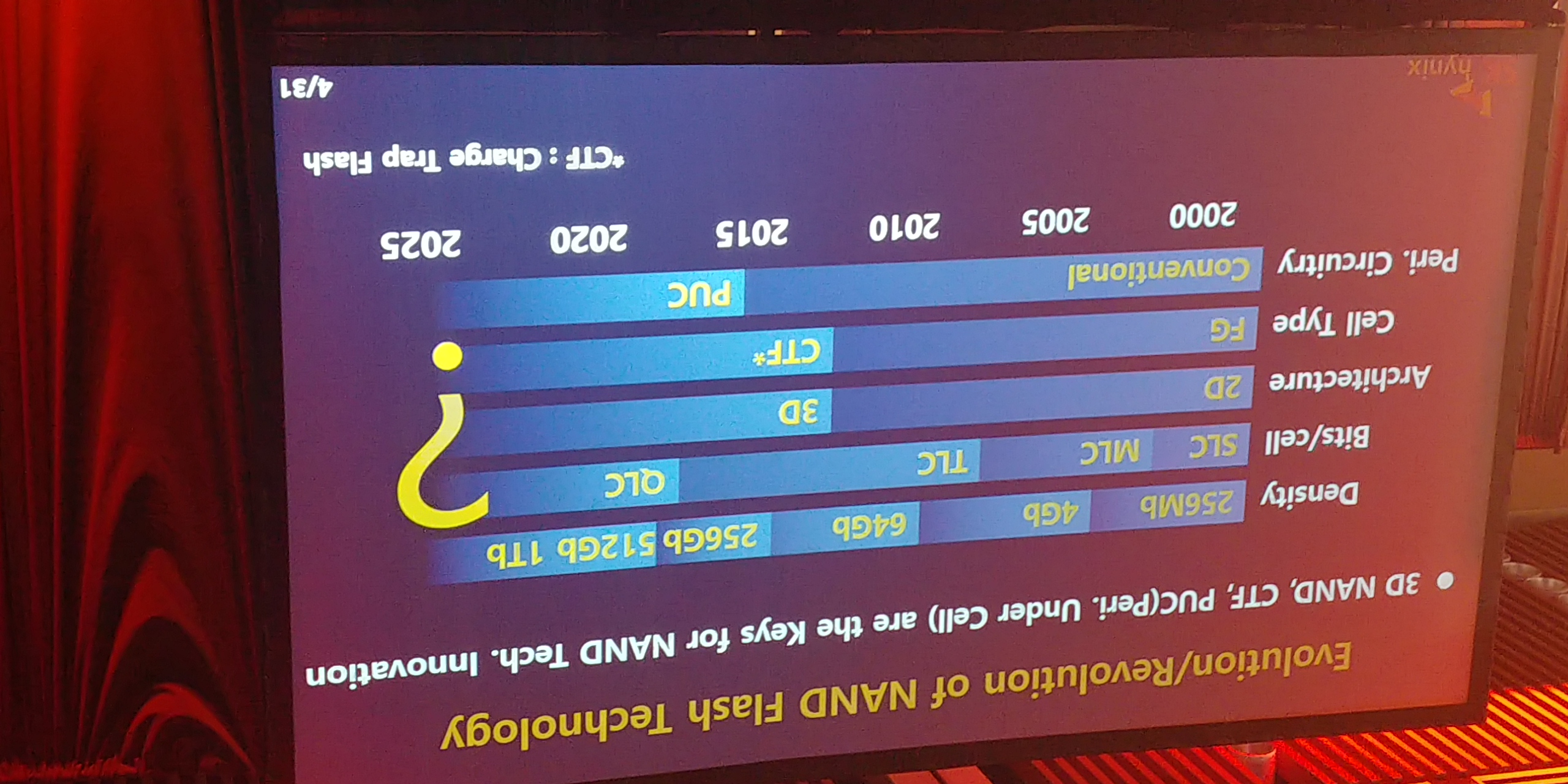
05:24PM EDT - one BGA package now has as much capaity as a whole wafer a decade ago
05:24PM EDT - Revolution of NAND. Increasing the density through 3D NAND, CRG, PUC
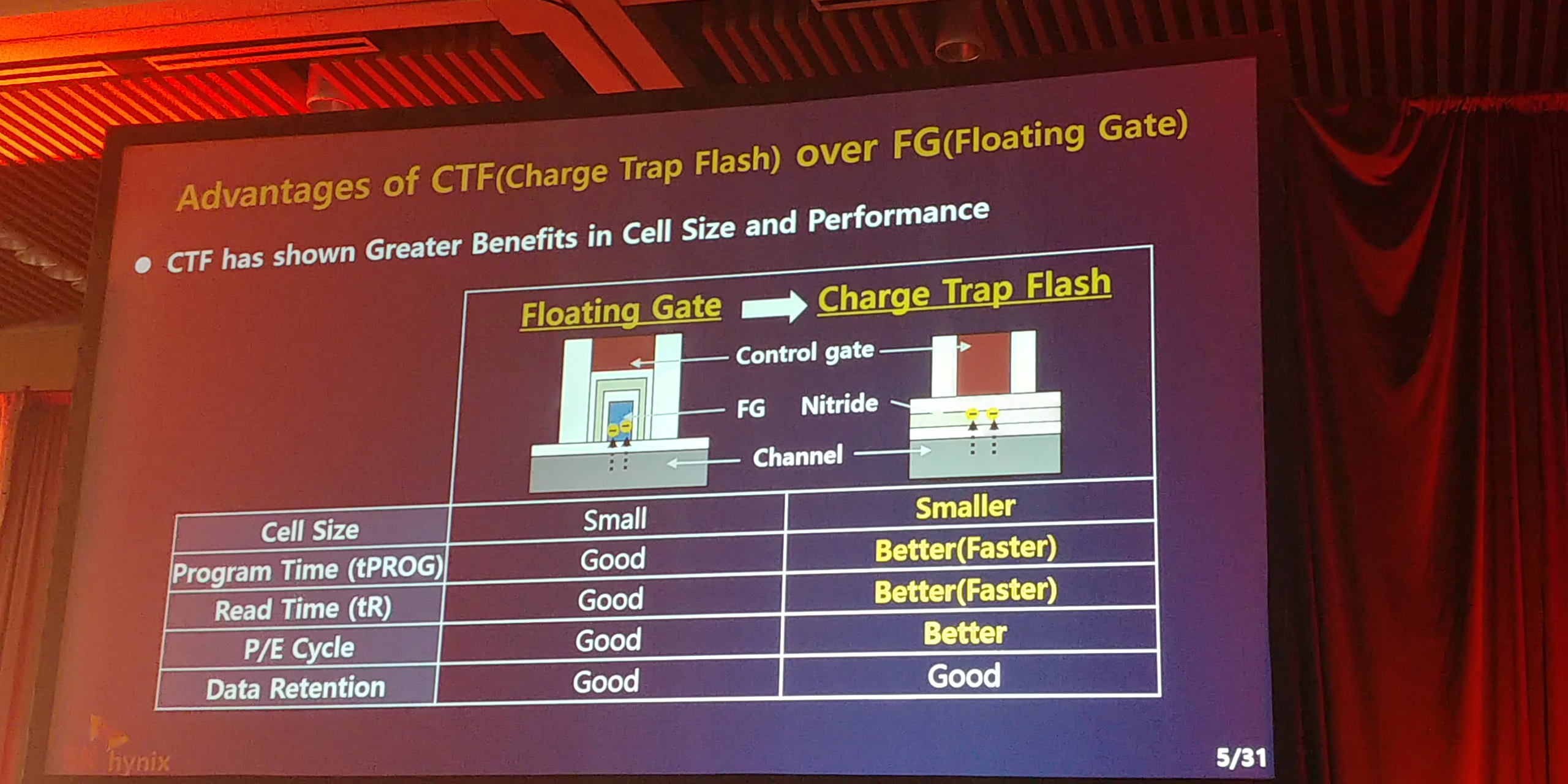
05:25PM EDT - Charge Trap Flash advantages over floating gate
05:25PM EDT - Smaller cells, better programming time, better read time, better P/E cycles
05:26PM EDT - Differences in structure depends on where electrons are stored
05:26PM EDT - Isolate materials to store electrons
05:26PM EDT - Floating gate has structural limitations
05:26PM EDT - Nitride in CTF means no interference
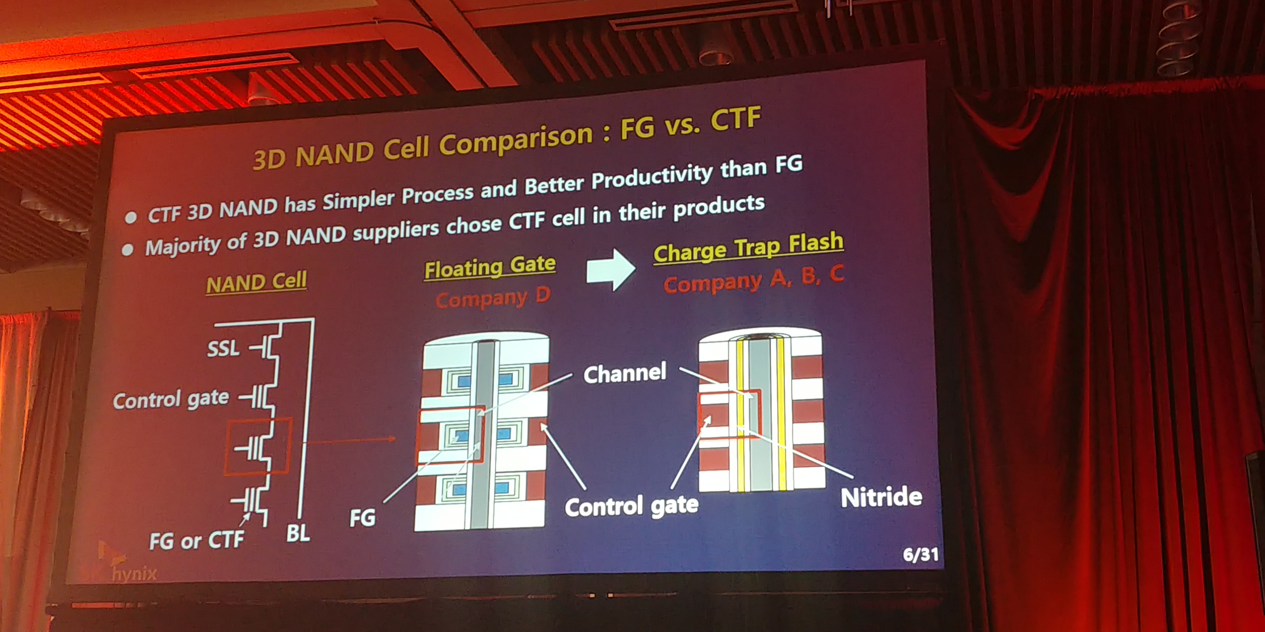
05:26PM EDT - process is simple and productivity is better
05:26PM EDT - Suppliers choose CTF for their products
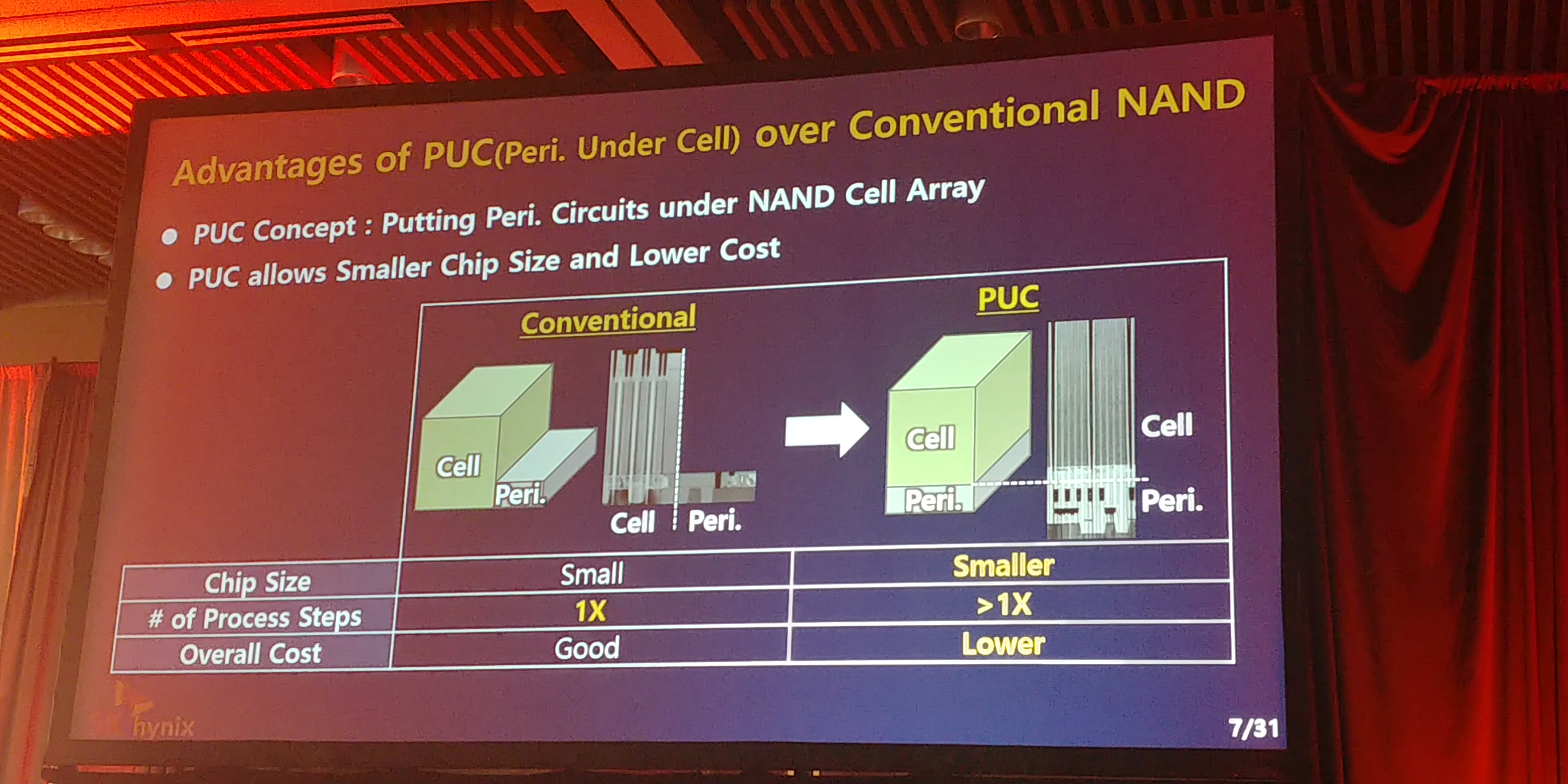
05:27PM EDT - PUC puts most of the circuits under the cell
05:27PM EDT - But requires more process steps
05:27PM EDT - Overall cost competitiveness, PUC wins
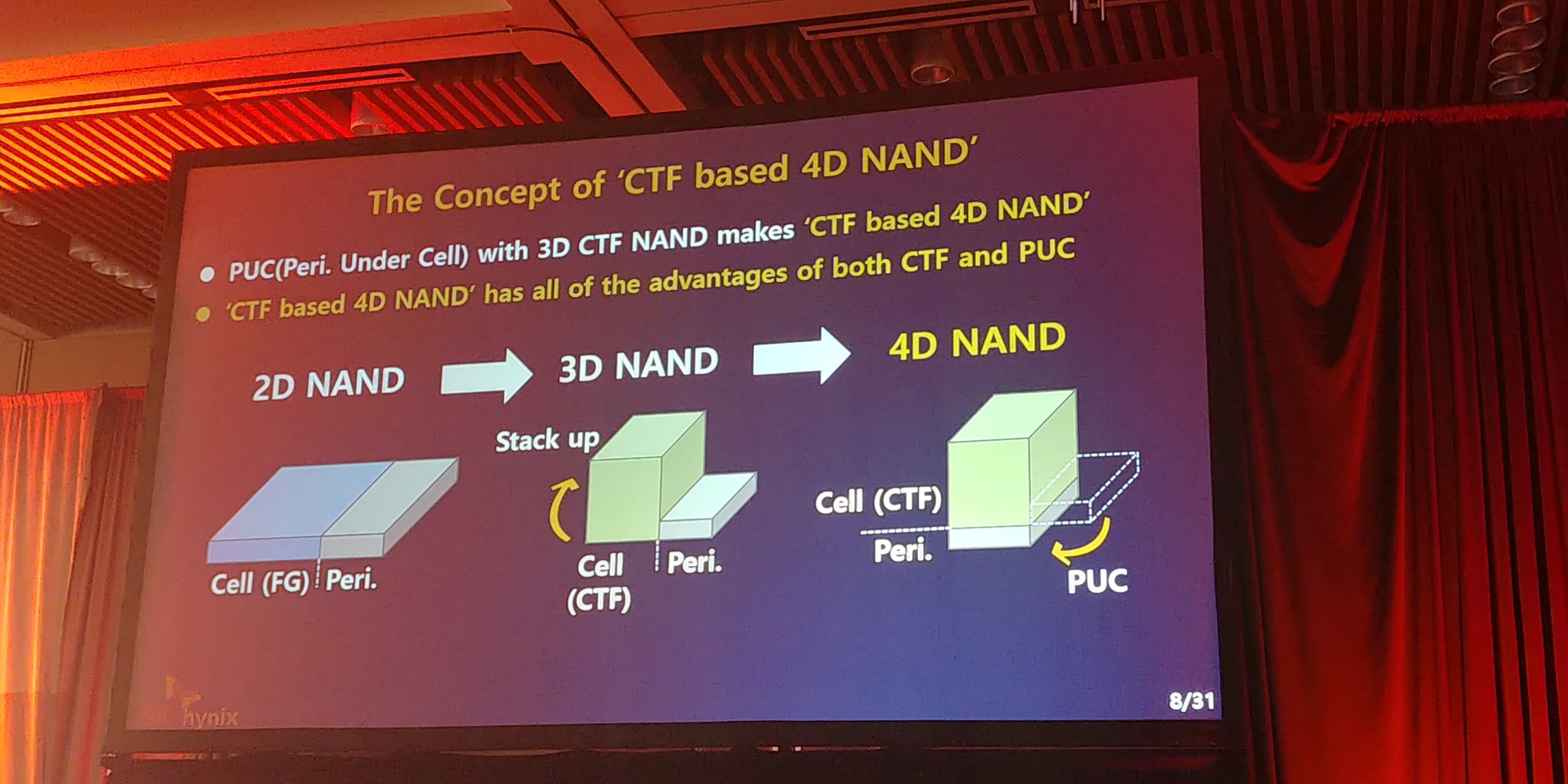
05:27PM EDT - 4D NAND = CTF + PUC
05:28PM EDT - (it's a very odd name)
05:28PM EDT - (Intel and Micron have been doing the equivalent of PUC since their first-generation 3D NAND)

05:28PM EDT - First 4D NAND - 96 stacks
05:28PM EDT - 512 Gb TLC product
05:28PM EDT - sampling from Q4 2018
05:28PM EDT - mobile package at 11.5 x 13.0 mm
05:29PM EDT - 1.2 Gbps/pin IO Speed
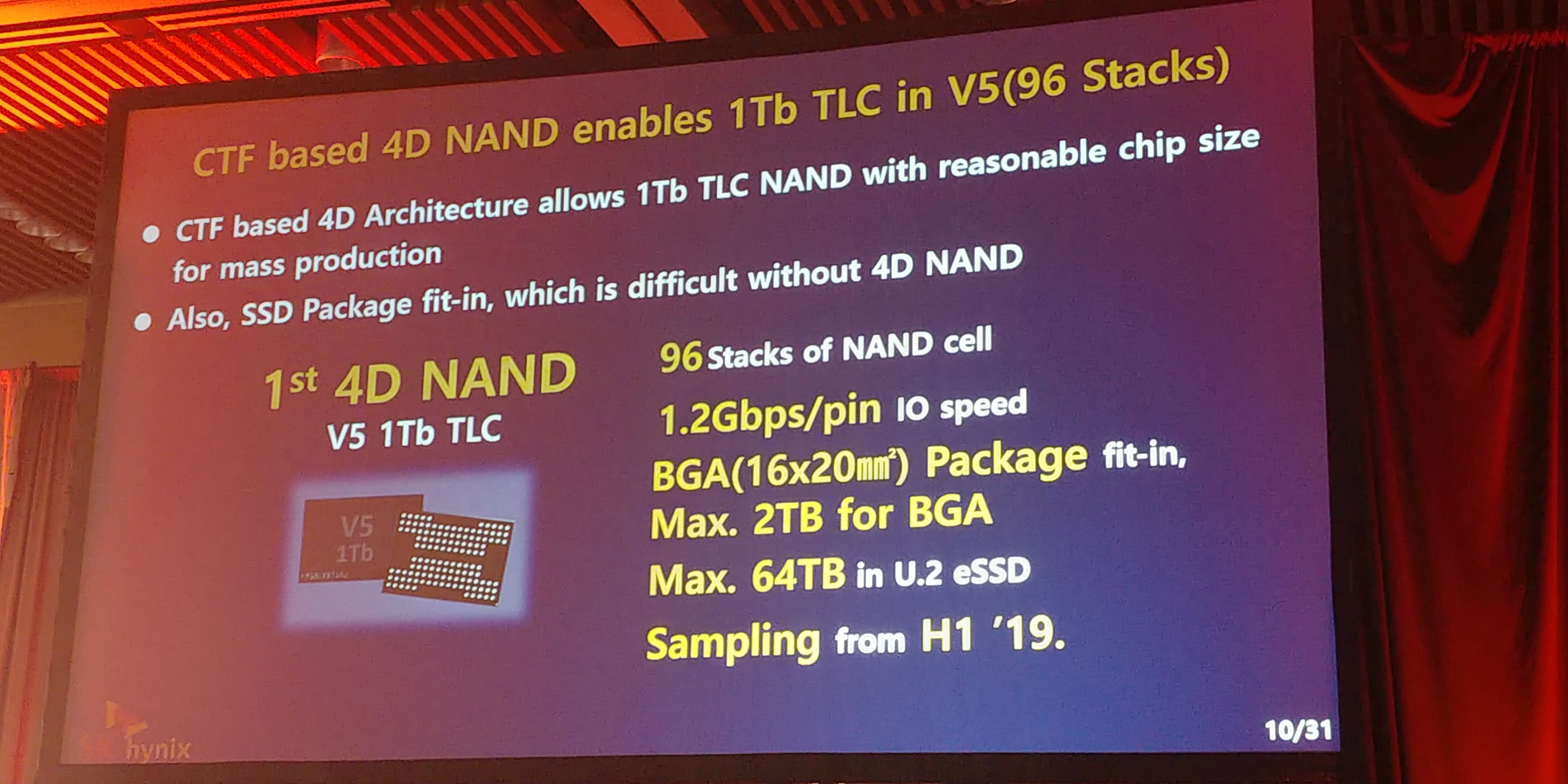
05:29PM EDT - Bigger BGA procuct for 1Tb TLC
05:29PM EDT - Max 2GB for BGA, Max 64TB in U.2
05:30PM EDT - Sampling from H1 2019
05:30PM EDT - V5 = version 5 ?
05:30PM EDT - or V5 is the product name
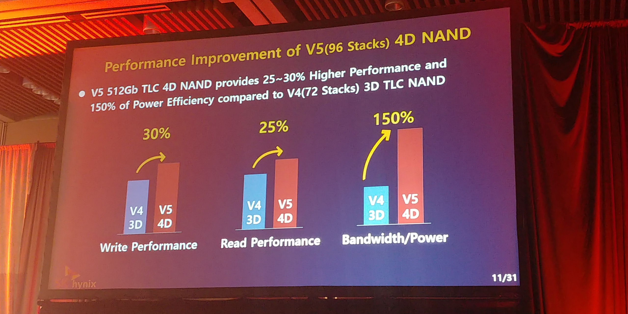
05:31PM EDT - +30% read perf, +25% write perf, 150% better Bandwidth/Power
05:31PM EDT - 96 lyaer vs 72 layer (v5 compared to v4)
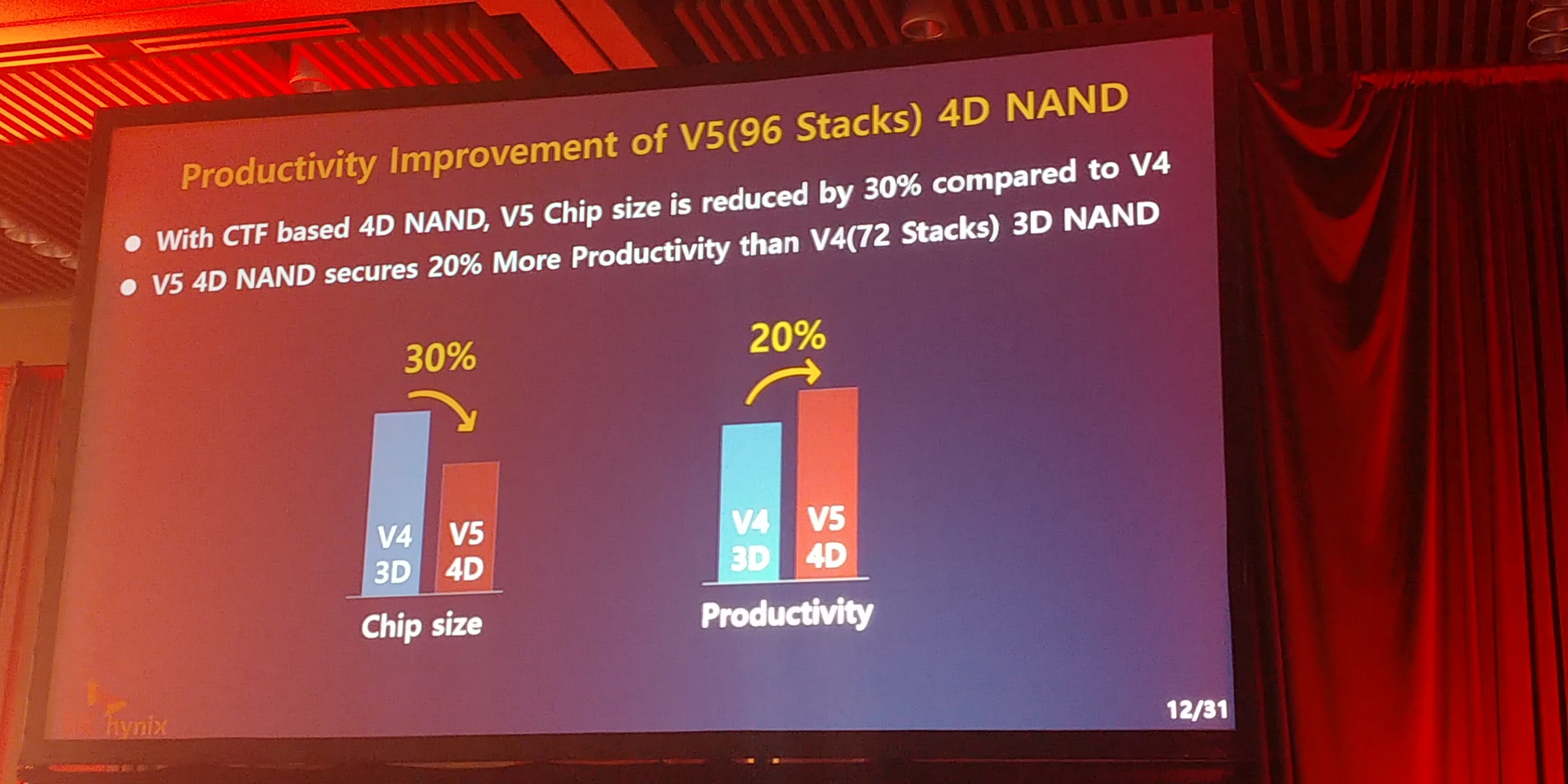
05:31PM EDT - 30% smaller chip size

05:32PM EDT - also looking at QLC
05:32PM EDT - 1Tb in mini die
05:32PM EDT - aiming for replacing near-line HDD
05:32PM EDT - Sampling in H2 2019
05:32PM EDT - Uses 4D NAND V5
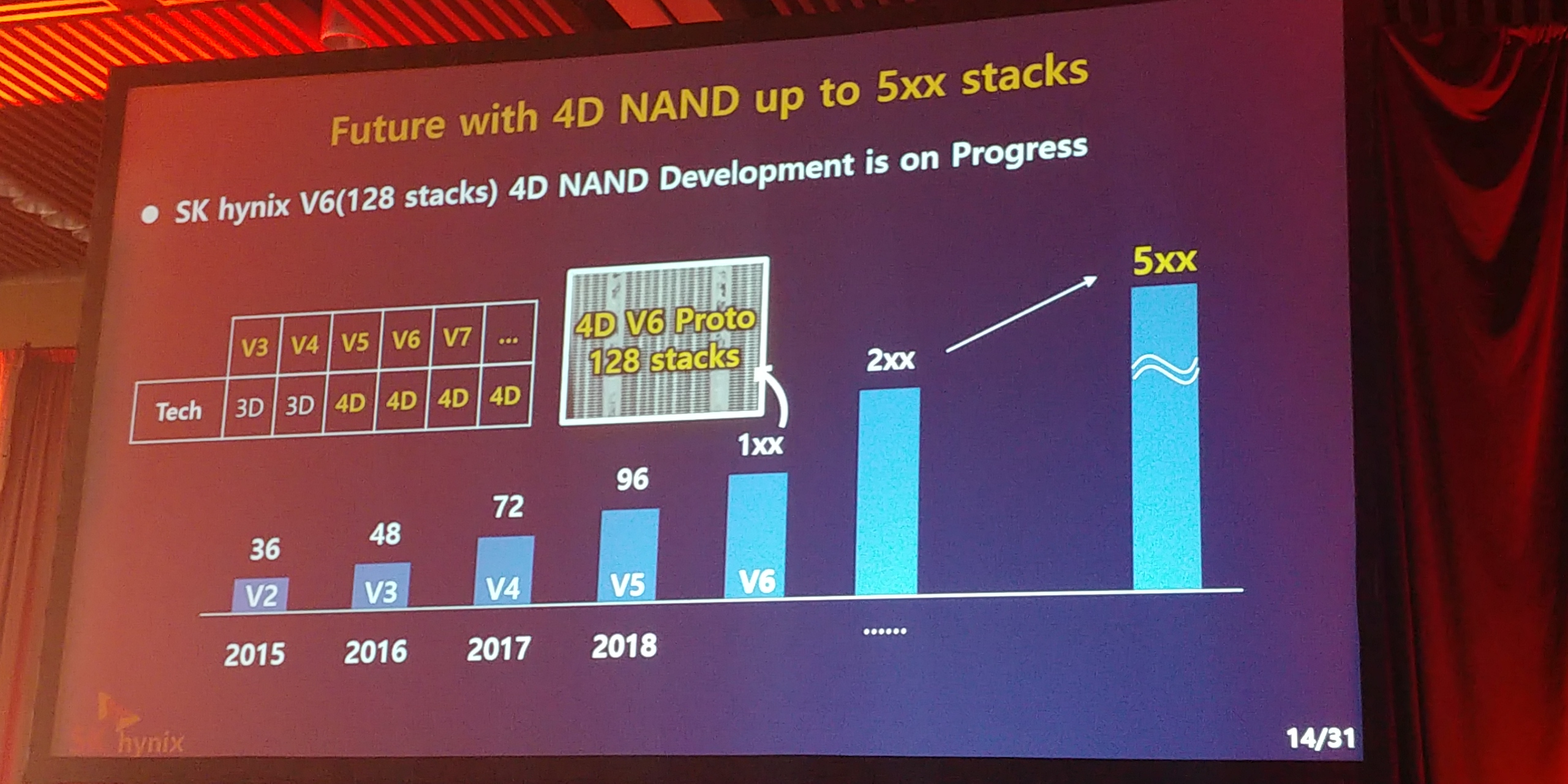
05:32PM EDT - Already working on 128 stacks in V6 product
05:32PM EDT - 1Tb QLC in 2H '19 means SK Hynix will continue to lag behind the other NAND manufacturers
05:33PM EDT - looking at over 500 stacks in the future
05:33PM EDT - (where's the 5D ?!? )
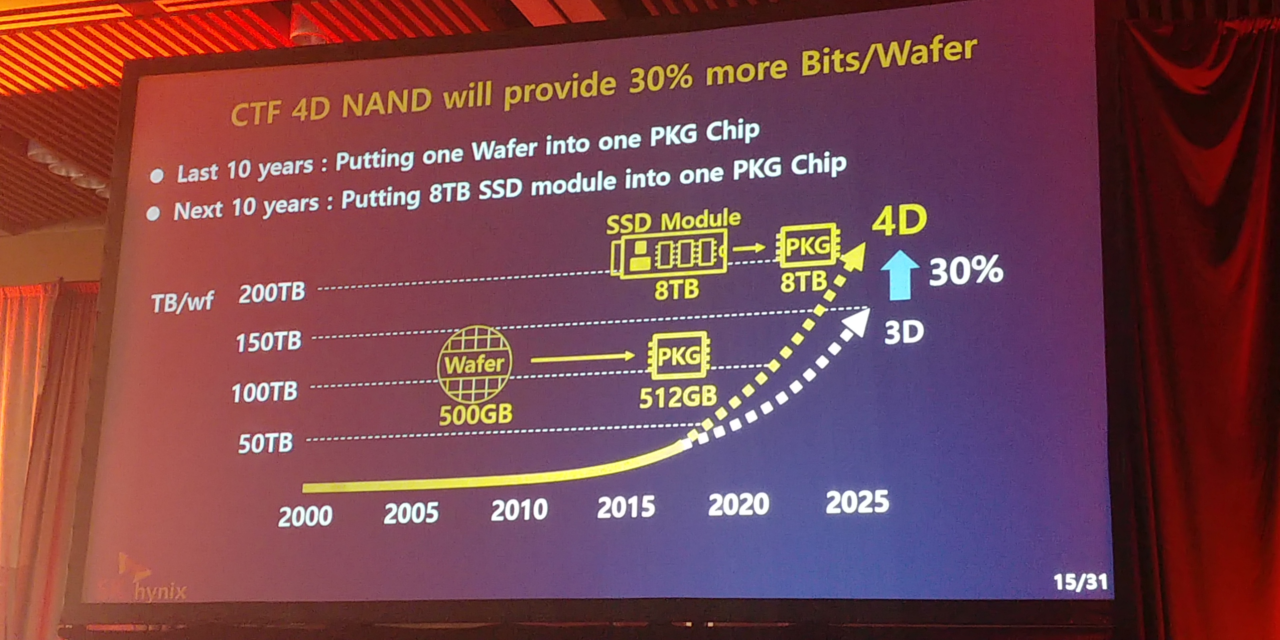
05:33PM EDT - Looking to put 8TB on one package chip by 2025
05:34PM EDT - y-axis is TB/wafer
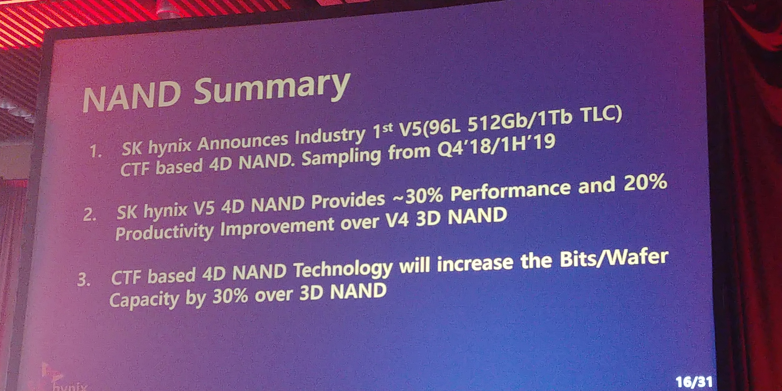
05:35PM EDT - So the news: 4D NAND in V5 product. 96 stacks, looking at 512Gb and 1Tb chips. Sampling by 2019
05:35PM EDT - Aiming for 500 stacks. CTF will get us there
05:35PM EDT - Next SK Hynix speaker
05:36PM EDT - Transitioning SK Hynix into a solutions company
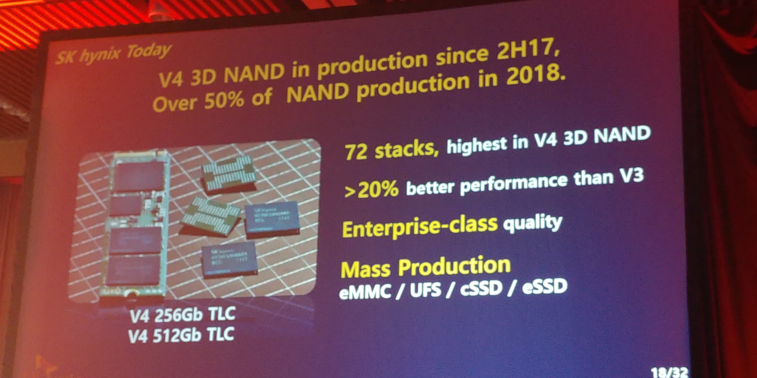
05:36PM EDT - In 2018, half of SK Hynix production will be 3D NAND V4
05:36PM EDT - +20% perf over V3
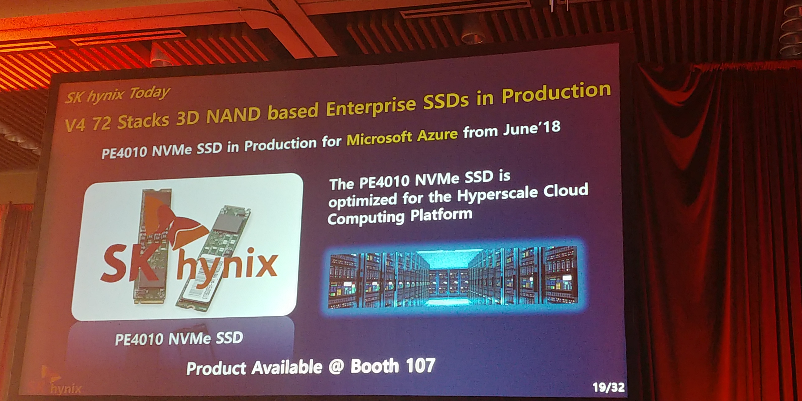
05:37PM EDT - SK Hynix own-brand Enterprise SSDs already in deployment in Azure
05:37PM EDT - PE4010
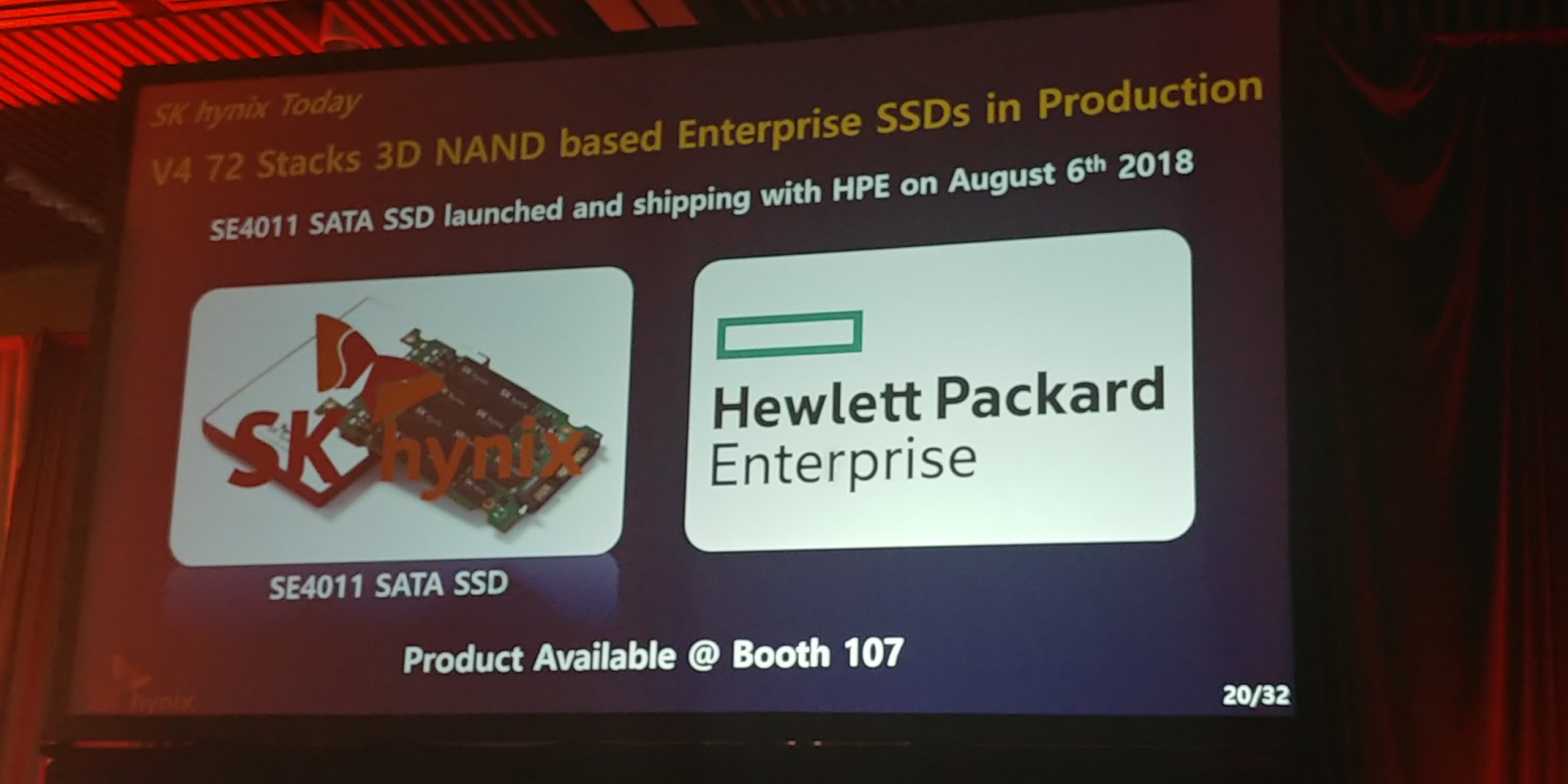
05:38PM EDT - Also SE4011 PCIe SSD deployed to HPE
05:38PM EDT - Also passed 1st phase of tencent eval in Q2 2018 with this SSD
05:38PM EDT - Sorry, SE4011 is a SATA SSD

05:39PM EDT - new NVMe SSD PE6000 sampling from Q4 2018
05:39PM EDT - 650K random read IOPS with 11W
05:39PM EDT - Dual Support
05:39PM EDT - U.2 form factor
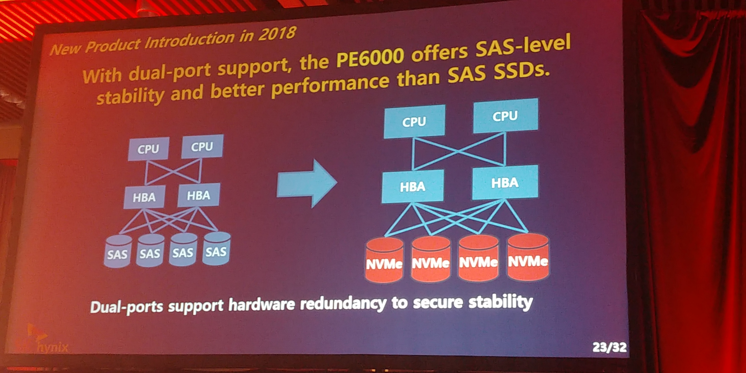
05:40PM EDT - all the enterprise-grade NVMe features: IO determinism, multi-streams, dual-port, NVM Sets
05:40PM EDT - Transition into a solution company
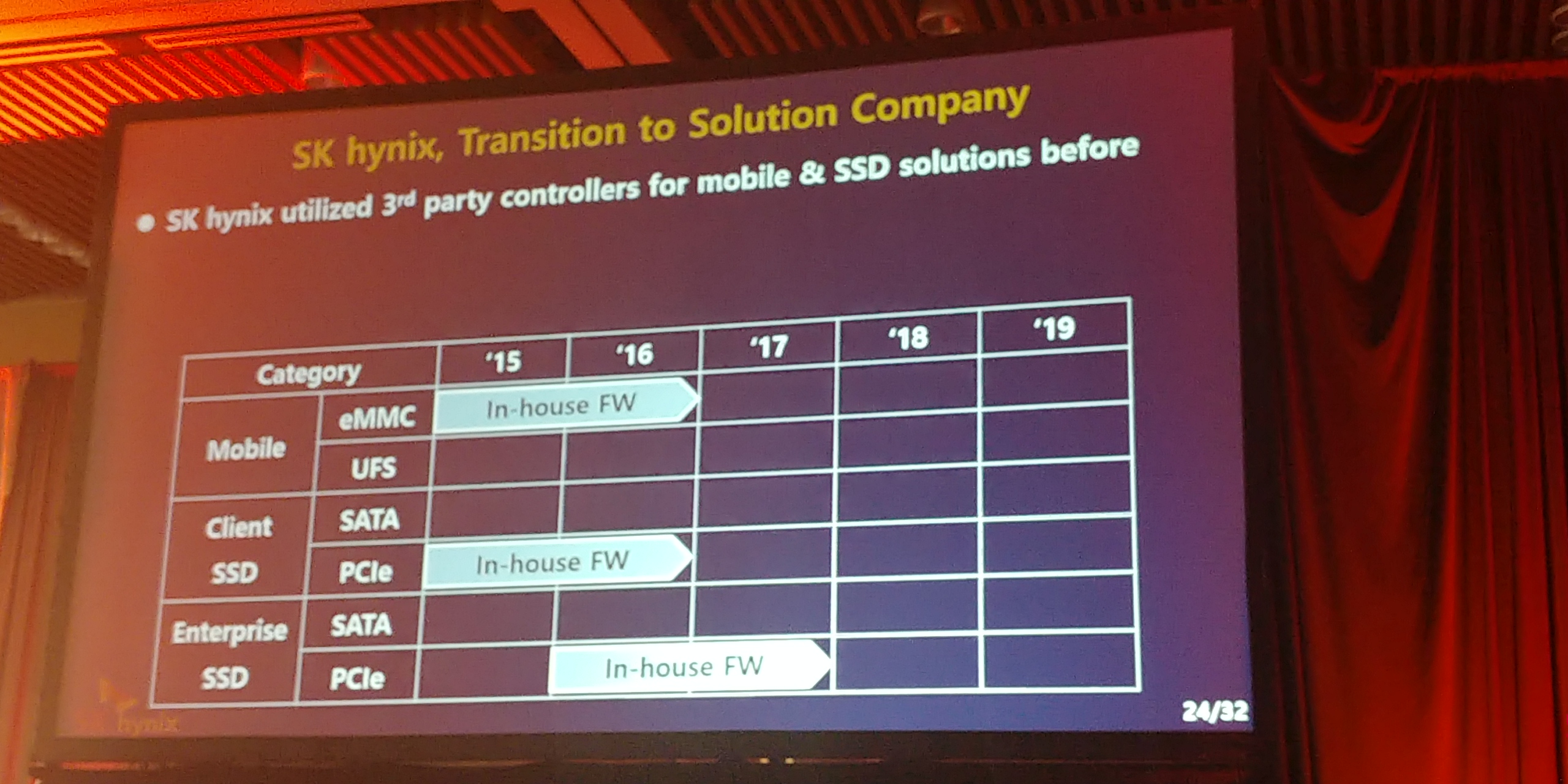
05:41PM EDT - firmware from top to bottom from 2019 with 4D NAND V5
05:41PM EDT - Now innovation in Next Storage Systems
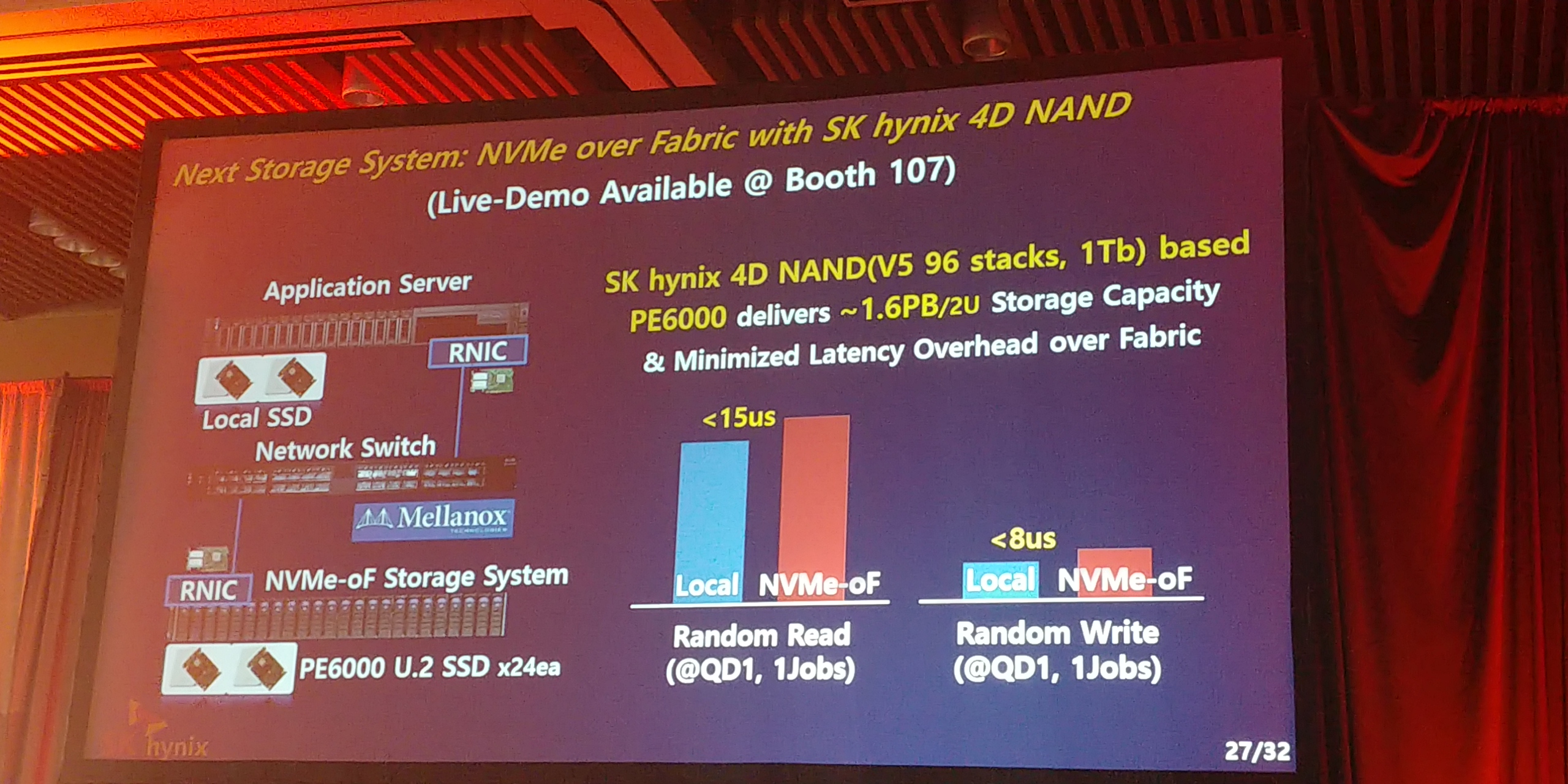
05:42PM EDT - NVMe-oF using 4D NAND 1Tb
05:42PM EDT - Demo on the show floor
05:43PM EDT - 1.6PB in a 2U
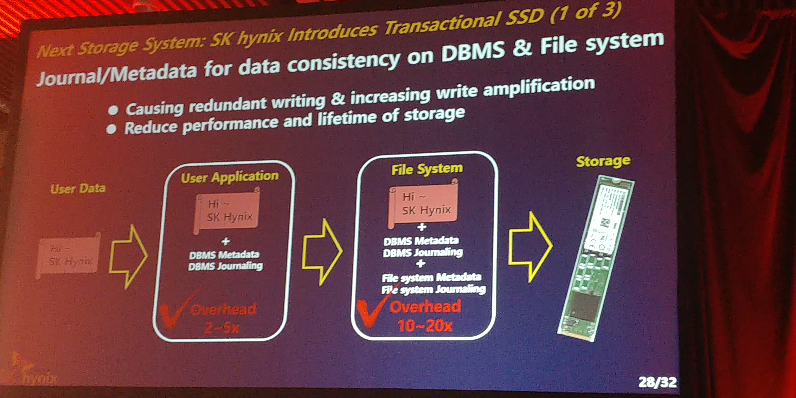
05:43PM EDT - Also developing fie systems
05:44PM EDT - Reducing write amplification
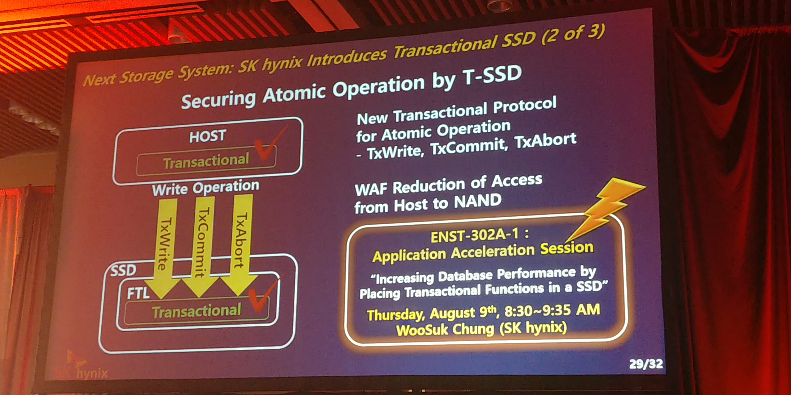
05:44PM EDT - New transactional protocol for atomic operations
05:44PM EDT - New API for storage operations to remove overhead
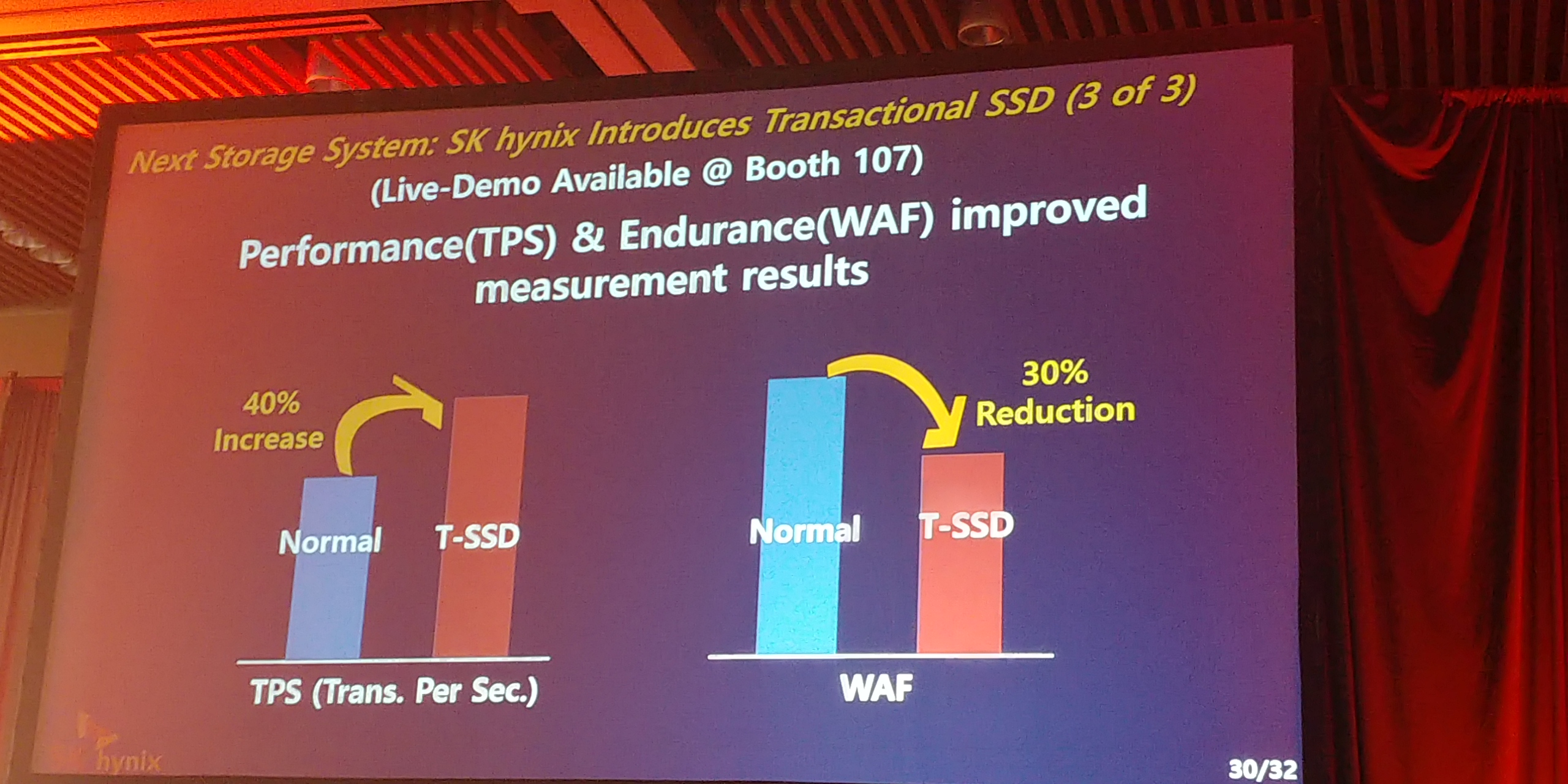
05:45PM EDT - Transactional SSDs
05:45PM EDT - 40% increase transactions per second, 30% reduction in writes (improvement in endurance)

05:46PM EDT - Didn't put a timeframe on Transactional SSD, but it seems to be aligned with 4D NAND

05:46PM EDT - SK Hynix is increasing in capacity
05:47PM EDT - Starting production in M15 in 2019. 250k wafer starts per month
05:47PM EDT - M16 fab cost $3B, construction complete in 2020
05:47PM EDT - That's a wrap. YMTC next!


1 Comments
View All Comments
iwod - Sunday, August 12, 2018 - link
Intel could fit 1PB inside 1U with its Ruler, I wonder if SK Hynix could do that instead of using U.2.So by 2025, we are looking at possible half of EB in a rack.