Qualcomm Reveals The Snapdragon 670 Platform: Dual Big Cores + Adreno 615
by Andrei Frumusanu on August 8, 2018 7:30 AM EST- Posted in
- Mobile
- Qualcomm
- Smartphones
- SoCs
- Snapdragon 670
Today Qualcomm is announcing a new entry in the 600-series mid-range line-up. In a surprise move, the new Snapdragon 670 is a direct successor to the Snapdragon 660, and is intended to fill the gap between the 600-series and the newly introduced Snapdragon 710.
As a quick refresher, the Snapdragon 710 was released this year as the first entry in the new Snapdragon 700 tier of SoCs. The 700 series is intended to sit between the existing 600 and 800 series, offering many of Qualcomm's flagship features at a lower cost, something that's been in demand from handset vendors who are looking at putting together high-performance phones for more price-conscientious buyers.
The new Snapdragon 670, in turn, seems to be directly derived from the 710, as the two are so close in specifications that at first glance it's easy to miss the differences.
| Qualcomm Snapdragon Upper Mid-Range SoCs | |||
| SoC | Snapdragon 660 | Snapdragon 670 | Snapdragon 710 |
| CPU | 4x Kryo 260 (CA73) @ 2.2GHz 4x Kryo 260 (CA53) @ 1.8GHz |
2x Kryo 360 (CA75) @ 2.0GHz 6x Kryo 360 (CA55) @ 1.7GHz |
2x Kryo 360 (CA75) @ 2.2GHz 6x Kryo 360 (CA55) @ 1.7GHz |
| GPU | Adreno 512 | Adreno 615 | Adreno 616 |
| DSP | Hexagon 680 | Hexagon 685 | |
| ISP/ Camera |
Spectra 160 ISP 24MP |
Spectra 250 ISP 25MP single / 16MP dual |
Spectra 250 ISP 32MP single / 20MP dual |
| Memory | 2x 16-bit @ 1866MHz LPDDR4 14.9GB/s |
2x 16-bit @ 1866MHz LPDDR4X 14.9GB/s 1MB? system cache |
|
| Integrated Modem | Snapdragon X12 LTE (Category 12/13) DL = 600Mbps 3x20MHz CA, 256-QAM UL = 150Mbps 2x20MHz CA, 64-QAM |
Snapdragon X12 LTE (Category 15/13) DL = 600Mbps 3x20MHz CA, 256-QAM UL = 150Mbps 2x20MHz CA, 64-QAM |
Snapdragon X15 LTE (Category 15/13) DL = 800Mbps 3x20MHz CA, 256-QAM UL = 150Mbps 2x20MHz CA, 64-QAM |
| Encode/ Decode |
2160p30, 1080p120 H.264 & H.265 |
2160p30, 1080p120 H.264 & H.265 |
2160p30, 1080p120 H.264 & H.265 10-bit HDR pipelines |
| Mfc. Process | 14nm LPP | 10nm LPP | |
The Snapdragon 670 uses the same CPU configuration as found on the Snapdragon 710. The new Kryo 360 performance and efficiency cores are based on Cortex A75 and A55 IP designs and come in a configuration of 2x big cores at 2.0GHz and 6x small cores at 1.7GHz. This is a slight 200MHz downgrade from the 710’s 2.2GHz cores. It’s to be noted that as a direct successor to the 660, we’re losing two big cores, so multithreaded performance might not see much of an upgrade on the new chip.
The GPU is also a new Adreno 6xx generation design in the form of a 615 implementation. Obviously we don’t know much at all from just the model number, but it being numerically inferior to the S710’s Adreno 616, performance should be slightly less. Qualcomm promises a performance increase of 25% over the Snapdragon 660, while the 710 promised a 35% increase in the same comparison.
The 670’s DSP and ISP are identical in terms of design to the 710’s – however they’re run at a lower clockspeed and subsequently support a lower maximum resolution.
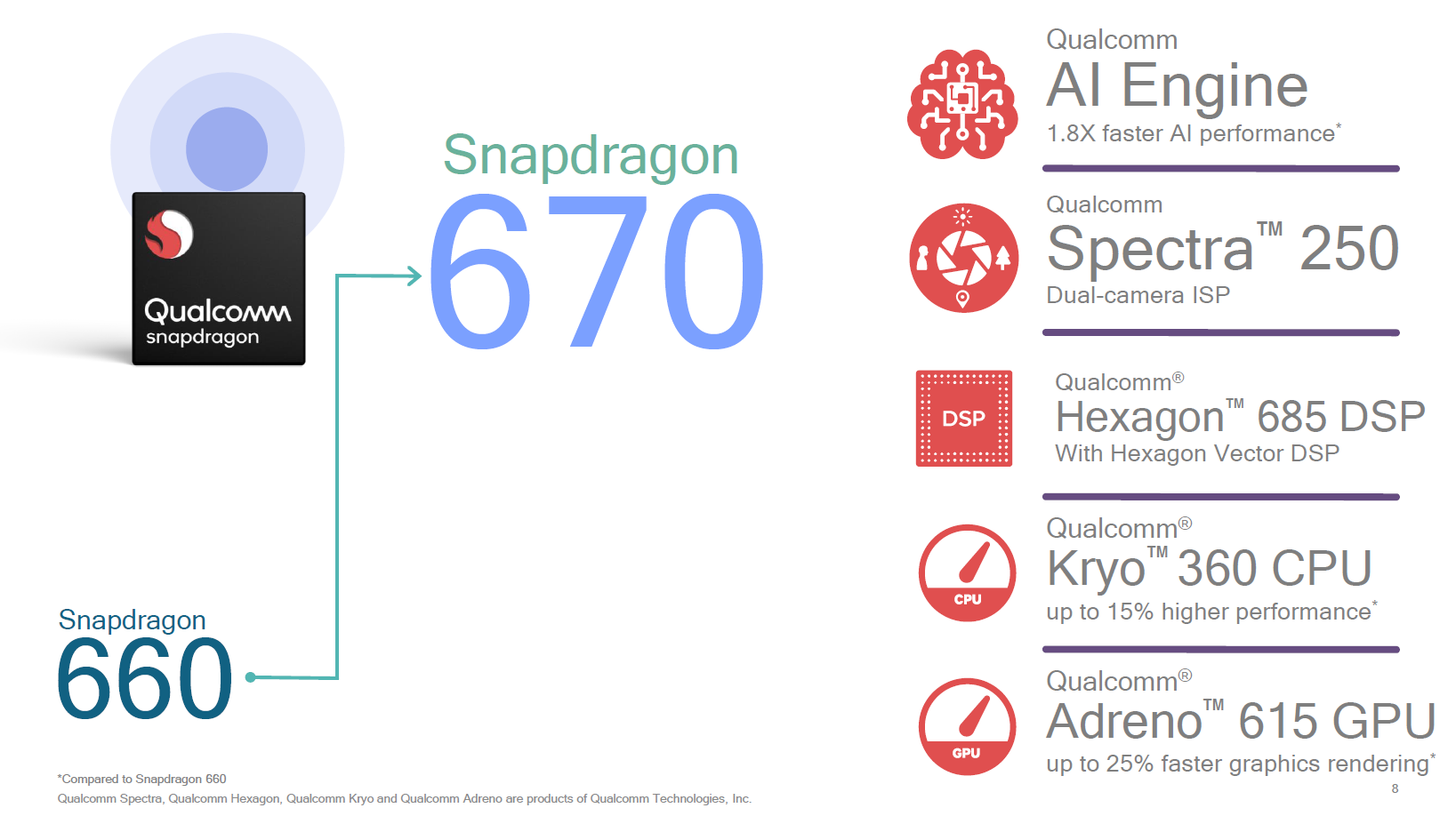
One of the other feature shavings is that the 670 doesn’t support 4x4 MIMO on the modem, and thus the X12 modem has a lower download speed of up to 600Mbps versus 800Mbps on the 710.
Finally, the other seemingly important discrepancy here is the lack of 10-bit display pipelines and accompanying support on the part of the encoders, so HDR capture isn’t a feature on the 670. The display controller also is less capable and only able to drive FHD+ resolutions as opposed to the QHD+ capabilitites of the 710.
Like the 710, the 670 is manufactured on a newer 10LPP process node, so it should benefit from the same power efficiency gains as its higher end sibling.
The Snapdragon 670 is a surprising chipset in terms of its positioning because it’s not that far off from the Snapdragon 710. When briefed about the new model the first thing I thought was if this would be actually just a lower binned 710 – but Qualcomm confirmed that this is indeed a "different design". The market at these lower ranges is extremely competitive, and while the 670 does seemingly allow itself to shed some feature, I have to wonder just exactly how much silicon is saved as well as die area reduced in order for Qualcomm to decide that it’s actually worth to design and tape out a product to fill this lower price point under the 710. Seemingly, customers must have had demand for it otherwise it wouldn’t exist, and in a sense, it shows Qualcomm’s strength in terms of being customer demand driven and adapting fast to the market.
The last advantage of the Snapdragon 670 in this aspect is that it’s pin and software compatible to the Snapdragon 710, allowing vendors to choose between them with minimal engineering efforts.
The Snapdragon 670 is currently available and commercial devices are expected within the coming months.
Related Reading
- Qualcomm Announces Snapdragon 710 Platform
- Qualcomm Announces Snapdragon 700 Series Platform: Carving Out A Niche for Sub-Premium
- The Snapdragon 845 Performance Preview: Setting the Stage for Flagship Android 2018
- Qualcomm Announces Snapdragon 660 & 630 Mobile Platforms: Better Connectivity, Camera, & Compute at 14nm


25 Comments
View All Comments
ToTTenTranz - Wednesday, August 8, 2018 - link
It really does look like just a lower-binned S710, despite Qualcomm's claims.quadrivial - Wednesday, August 8, 2018 - link
I'd guess that the image processor is lower clocked, so the resolution is lowered. Likewise, disabling the HDR pipeline wouldn't be hard. I'm less sure about the modem though. Is the X12 and X15 the same chip with a channel disabled?ToTTenTranz - Wednesday, August 8, 2018 - link
On paper, both Cat 12 and Cat 15 use the same amount of MIMO layers, and Cat 15 gets 25% higher DL speeds. I have no real knowledge on this, but it could be that Cat 12 is achieved simply through a lower-clocked baseband processor.Spunjji - Thursday, August 9, 2018 - link
Hooray for bizarrely fine-grained Intel-style product segmentation!eastcoast_pete - Saturday, August 11, 2018 - link
Agree, it looks like Qualcomm found a way to "recycle" lower-binned S710s. Probably learned that from Intel, as another comment here said. Also, might be one of the signs of a "maturing" (read: slower growing) market. The Android universe is not expanding as fast as it used to be, and things like mini- and micro-segmenting are signs of it.psychobriggsy - Wednesday, August 8, 2018 - link
"different design"IMO that doesn't necessarily mean different silicon. It's so similar that would be silly.
To be honest, it looks like a 710 that couldn't make the 2.2GHz speed grade - i.e., a yield increasing SKU.
Valantar - Wednesday, August 8, 2018 - link
I agree. Also, it's about time that mobile SoC makers start selling different bins of chips. I know they've been doing this on the dl in terms of giving favored/higher-paying OEMs faster bins, but there still should be some way of selling partially-defective or not-up-to-spec silicon. Anything else is just plain wasteful. I get that these chips are mostly tiny and thus they get a lot of chips per wafer, but so what? Sell them cheaper and someone will inevitably buy them.Mil0 - Wednesday, August 8, 2018 - link
You say tiny, but I think they're not *that* tiny. I'd say 30-50 mm2, since 845 is 91mm2 on the same process. So optimistically 3x as much per wafer - selling partially defective/not up to spec silicon does seem like the smart thing to do. The modem is also (to me at least) surprisingly big, so lopping of part of that seems to make sense. (as in - disabling non-functional parts)Arnulf - Thursday, August 9, 2018 - link
Analog passive components don't scale with node changes the way transistors do in sillicon.ZolaIII - Wednesday, August 8, 2018 - link
Most of the type out is the same, untouched. It's questionable even did they even root modem DSP, RF front end is obviously different but that really isn't on the 10nm FinFET chip.