Huawei Server Efforts: Hi1620 and Arm’s Big Server Core, Ares
by Ian Cutress on November 20, 2018 11:00 AM EST- Posted in
- CPUs
- Arm
- Huawei
- Trade Shows
- Enterprise CPUs
- Ares
- Supercomputing 18
- Hi1620
For at least four years now, Arm has been pushing its efforts to be a big part of the modern day server, the modern day data center, and in the cloud as a true enterprise player. Arm cores are found in plenty of places in the server world, with big deployments for its smartphone focused Cortex core family in big chips. However, for those same four years, we have been requesting a high-performance core, to compete in single threaded workloads with x86. That core is Ares, due out in 2019, and while Arm hasn’t officially lifted the lid on the details yet, Huawei has already announced it has hardware with Ares cores at its center.
Huawei Is A BIG Company
Normally at AnandTech when we discuss Huawei, it is in the context of smartphones and devices such as the Mate 20, or smartphone chips like the Kirin family. These both fall under Huawei’s ‘Consumer Business Group’, which accounts for just under half of the company’s revenue. One of Huawei’s other groups is its Enterprise wing, which is almost as big, and it creates a lot of custom hardware and silicon using its in-house design team, HiSilicon. HiSilicon’s remit goes all the way from smartphones to modems to SSD controllers to PCIe controllers and also high-performance enterprise compute processors.
...And It Makes Server CPUs
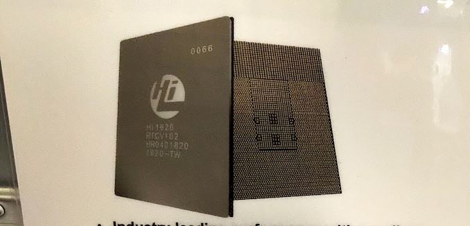
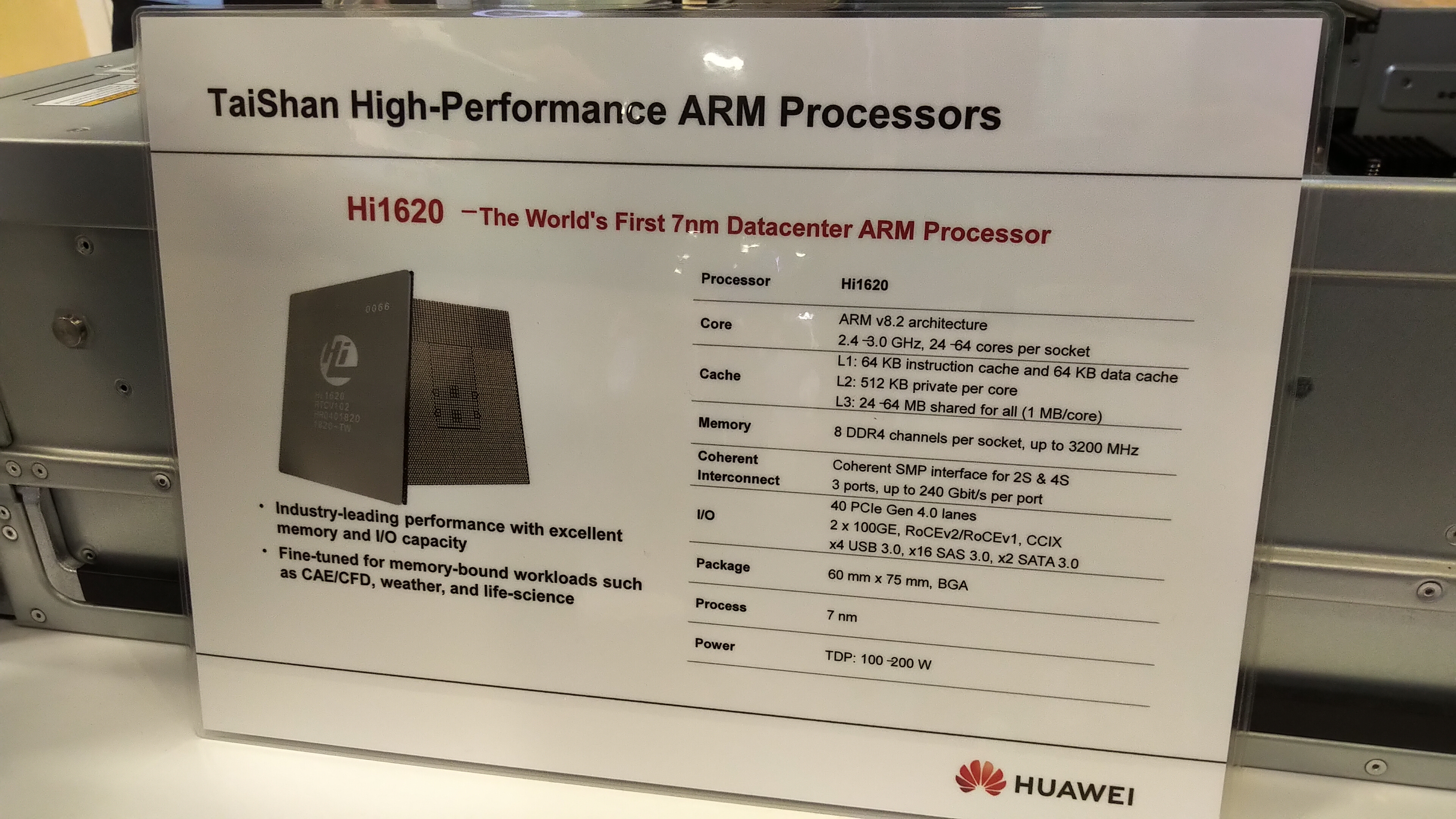
Last month, Huawei’s Enterprise Group lifted the lid on its fourth generation data center processor. Part of the TaiShan family, the Hi1620 would follow hardware such as the Hi1616 in being built using Arm IP. The new Hi1620 was announced as the world’s first 7nm processor for the data center, with the Ares cores being what would drive high-performance for its deployments.
While Huawei didn’t have any Hi1620 at the show, it was promoting the fact that it will be a cornerstone in its portfolio, and lifted the lid on a number of key parts of the chip.
| Huawei Hi16xx Family | ||||
| Hi1620 | Hi1616 | Hi1612 | Hi1610 | |
| Announced | 2018 | 2017 | 2016 | 2015 |
| Cores | 24 to 64 | 32 | 32 | 16 |
| Architecture | Ares | Cortex-A72 | Cortex-A57 | Cortex-A57 |
| Frequency (GHz) | 2.4 to 3.0 | 2.4 GHz | 2.1 GHz | 2.1 GHz |
| L1 | 64 KB L1-I 64 KB L1-D |
48 KB L1-I 32 KB L1-D |
48 KB L1-I 32 KB L1-D |
48 KB L1-I 32 KB L1-D |
| L2 | 512 KB Private | 1MB/4 cores | 1MB/4 cores | 1MB/4 cores |
| L3 | 1MB/core Shared | 32MB CCN | 32MB CCN | 16MB CCN |
| Memory | 8x DDR4-3200 | 4x DDR4-2400 | 4x DDR4-2133 | 2x DDR4-1866 |
| Interconnect | Up to 4S 240 Gbps/port |
Up to 2S 96 Gbps/port |
? | ? |
| IO | 40 PCIe 4.0 2 x 100 GE |
46 PCIe 3.0 8 x 10GE |
16 PCIe 3.0 | 16 PCIe 3.0 |
| Process | TSMC 7nm | TSMC 16nm | TSMC 16nm | TSMC 16nm |
| Power | 100 to 200 W | 85W | ? | ? |
The new Hi1620 will feature 24-64 cores per socket, running from 2.4-3.0 GHz. Each of these cores will have a 64KB L1-Data cache and a 64 KB L1-Instruction cache, with 512KB of private L2 cache per core. L3 would run at 1MB/core of shared cache, up to 64MB. On a scale of a consumer Skylake core, that means more L2 cache per core, but less L3. No word on associativity, however. One of the key question marks is on performance: a lot of vendors are hoping for an Arm core with Skylake-levels of raw performance.
Memory is set at 8 channels up to DDR4-3200, and the chip will support a multi-socket configuration up to 4S, with the coherent SMP interface capable of 240 GB/s for each chip-to-chip communication. The 4S layout would be a fully connected design.
IO for the Hi1620 is set at 40 PCIe 4.0 lanes, which is less than the 46 lanes on the Hi1616, but those ones were rated for PCIe 3.0. The Hi1620 will also have CCIX support, as well as dual 100GbE MACs, some USB 3.0, and some SAS connectivity.
The package listed is 60x75 mm BGA, which gives no real indication to the chip inside. But that’s a lot of balls on the back, and the package is larger than the 57.5x57.5 mm design from the last generation. Huawei states that the Hi1620 will be offered in TDP ranges from 100W to 200W, with the varying core count, but chips will be offered that can be fine-tuned for memory bound workloads.
There are still plenty of unanswered questions, such as the interconnect, but we really want to get to grips with the microarchitecture of Ares to see what is under the hood. A number of journalists at the show were predicting that Arm should be having an event in the first half of 2019 to lift the lid on the design of the core.
Related Reading
- Just When You Thought It Was Dead: Qualcomm Centriq Arm Server Systems Spotted
- Assessing Cavium's ThunderX2: The Arm Server Dream Realized At Last
- AppliedMicro's X-Gene 3 SoC Begins Sampling: A Step in ARM's 2017 Server Ambitions
- Investigating Cavium's ThunderX: The First ARM Server SoC With Ambition


11 Comments
View All Comments
abufrejoval - Tuesday, November 20, 2018 - link
Wow! Sure makes the EU processor seem like a late phantom d'opera...name99 - Tuesday, November 20, 2018 - link
What strikes me as interesting here is the pace of improvement. Mock Huawei all you like, but (like Apple) they are clearly on a schedule that targets serious meaningful improvement and innovation every year.How does Intel, purveyor of essentially the same system today as in 2015, expect this to end in the long run? Admittedly Huawei can't create cute code names as rapidly as Intel, but I suspect customers will care less about that than about these other improvements. Sure, like Apple, TODAY these systems are for Huawei internal use. But things change...
mode_13h - Wednesday, November 21, 2018 - link
What strikes me as interesting here is how deeply in bed ARM seems to have been with Huawei. Much of this tech, like Ares and CCIX, is stuff Huawei is probably getting from ARM - not building on its own.Are there any non-Chinese partners currently using their Ares cores?
> How does Intel, purveyor of essentially the same system today as in 2015
How can you say that? Beyond things like Skylake SP and Xeon Phi (which, although it's being wound down, is a testament to their attempts to adapt), they're working on dGPUs, a few lines of deep learning chips, and different integrations of FPGAs. Not to mention Optane.
About the only thing you can't accuse Intel of doing, lately, is resting on their laurels. They seem as aware as anyone of what they stand to lose. You can fault their execution in several areas, but I don't think you can seriously accuse them of complacency.
Death666Angel - Wednesday, November 21, 2018 - link
Paranoid much?mode_13h - Friday, November 23, 2018 - link
WTF?Meteor2 - Monday, November 26, 2018 - link
Intel is the absolute archetype of modern-day corporate complacency. They thought they had microprocessing sown up, slashed R&D, and failed to see what was coming at them full steam.Do you really think a few FGPAs and a niche memory type will make up for the loss of their CPU business?
Kevin G - Monday, January 7, 2019 - link
Diversification can help a company weather through a storm that takes out their cash crop. In the case of Intel, yes, FPGA and Optane can help the company weather the CPU threat in the server area from AMD, ARM and IBM/nVidia. What is worrisome is that Optane DIMMs are late (supposed to launch alongside Sky Lake-SP but delayed due to errata). Their FGPA road inherited from Altera has been steady with the exception of the combo Xeon + FPGA parts. There is the Gold 6138P and some prototypes floating around under NDA. The idea of putting an FPGA into a Xeon package predates Intel buying Altera. Cascade Lake and Intel finally pushing out 10 nm chips in volume will address these two concerns this year.Intel also has their Nervena accelerators coming this year can be another pillar to support the company when during the increased time of CPU competition.
peevee - Wednesday, November 21, 2018 - link
"Arm core with Skylake-levels of raw performance"What is "raw performance"? Adding 2 AVX (or NEON for ARM) registers to each other on 64 cores in a loop gives you one performance, real life usually something 100 times lower, simply because to do anything actually useful it needs to read and write memory (and fight starts on 1st shared cache actually, not even memory), and mostly in patterns very different from what those vector instructions suppose...