Arm Announces Cortex-A65AE for Automotive: First SMT CPU Core
by Andrei Frumusanu on December 18, 2018 9:00 AM EST- Posted in
- CPUs
- Arm
- SoCs
- Automotive
- Cortex A65
- Cortex A65AE

Back in September, Arm had announced the new Cortex A76AE CPU with focus on automotive applications. Today, Arm adds to its portfolio by formally announcing a next gen processor with simultaneous multithreading, the new Cortex A65AE.
The previously announced A76AE CPU was Arm’s first to feature the “split-lock” technology that allowed two CPU cores to operate in a configurable lock-step operation mode, allowing the units to process tasks in parallel to each other and compare results for discrepancies – achieving a required level of functional safety of the software that is run on the system.
The Cortex A76AE was pretty much focused on heavy compute tasks and thus also fully takes advantage of the new high performance that is delivered by Arm’s new microarchitecture that came out of the Austin design centre. During the reveal of the A76AE, there were mentions of a “Helios” CPU core – to date it wasn’t too clear what this was meant to be, but it very much seemed like a new class of core that was meant to accompany the A76AE.
The Arm Cortex A65AE
Today, Arm finally formally announces the new Cortex A65AE, and although today’s material isn’t a full technical disclosure of the new CPU core, it does finally shed a little bit of light of what Helios is meant to be.
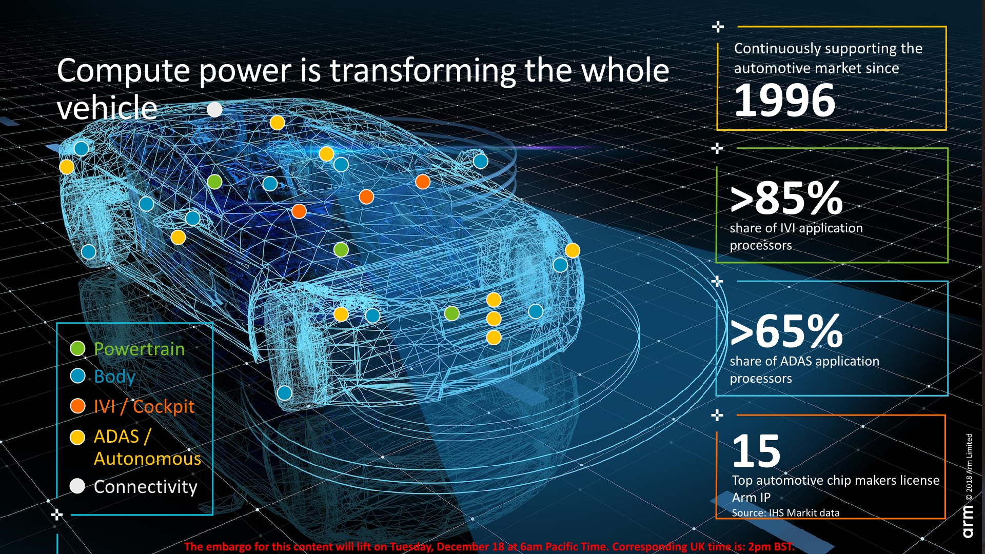
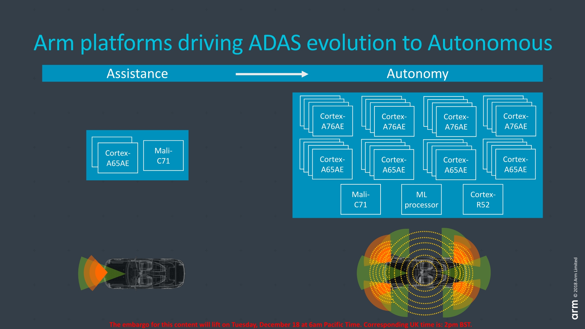
Much like during the Cortex A76AE release, Arm talked quite a bit about the needs of the automotive market and how cars are becoming increasingly demanding in terms of their need for compute power. Every single part of a car is becoming increasingly computerised, and advances in ADAS and future autonomous applications will explode the amount of processing power needed.

While the Cortex A76AE was focused on applications where high performance is needed, the Cortex A65AE is focused on high-throughput applications. The difference here would be in a sense the difference between demanding single-threaded workloads and demanding highly parallel and numerous multi-threaded workloads. Of the latter scenario, Arm emphasises the requirement of sensor processing in autonomous driving. Here the amount of sensors in a car is said to massively increase, and with it, also the need for higher throughput processing power.
Arm’s First SMT CPU Microarchitecture
Today’s announcement is a bit of an odd one in that we're talking about something important like Arm's first SMT microarchitecture as part of a more mundane automotive IP announcement, and yet the use-case presented here is the perfect fit for it. The Cortex A65AE is Arm’s first multi-threaded CPU core, allowing two threads to be executed per core. At the moment Arm is being very tight-lipped about the details of the microarchitecture, but they were able to comment on a bit of background information of the core.
As we’ve explained in the past, Arm usually has three main design centres which design the Cortex-A lineup of cores: The Cambridge team (A53, A55), the Sophia-Antipolis team (A73, A75), and the Austin team (A57, 72, and the new A76 family). The most interesting aspect of the Cortex A65AE is its heritage: although it was initially started by the Cambridge team, it then became a joint project and then finally finished to production quality by Arm’s newest team in their Chandler design centre in Arizona, making this effectively the first project coming out of this new team.
The reason why I dug into where the core came from is that it gives us greater perspective into what the microarchitecture might look like. Arm was able to disclose that this is indeed an out-of-order CPU core with SMT, but that’s about it in terms of what they were willing to reveal. The fact that the design started in Cambridge very much hints that this is somehow related to previous little cores such as the Cortex A53 and A55 – but the addition of OoO and SMT does make it seem more of distant cousin rather than a successor.
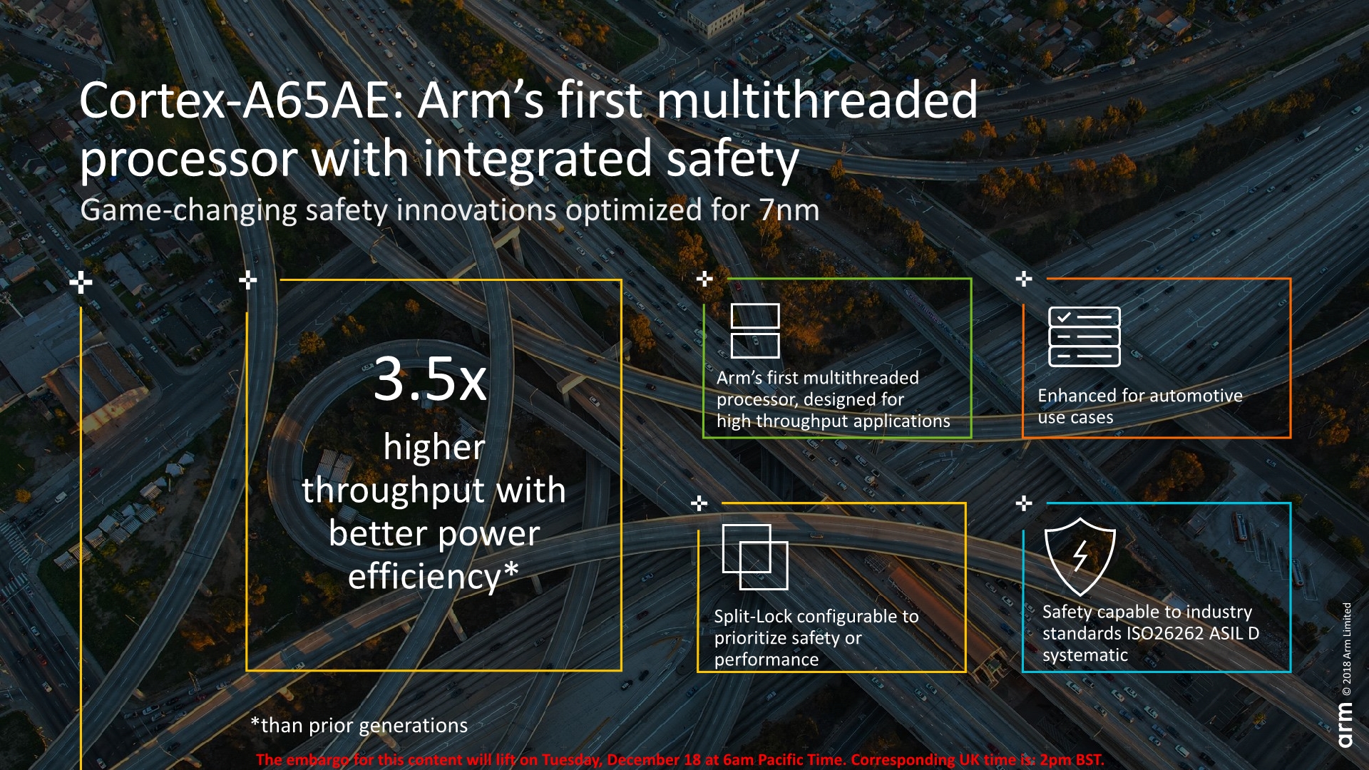
The only performance figure publicised during the presentation is the fact that the new CPU core is advertised as having a 3.5x higher throughput than the prior generation core in the same market segment – in this case a Cortex-A53. Arm usually makes performance projections based on the process node that an IP will typically be built on, again in this case that would be 7nm. Assuming a best-case scenario of 1.8-2x increased throughput through SMT, it still leaves quite a hefty difference that could be accounted for by frequency increases through the process node, or simply IPC improvements to the microarchitecture.
Again, the main benefit of the inclusion of SMT comes from the fact that in the primary automotive use-case of the Cortex A65AE, we’ll be seeing a load of sensors all communicating simultaneously to the central control unit of a car.
Arm’s SMT implementation also looks to be unique in terms of its functional safety features: Much alike “Split-Lock” mode on the Cortex A76AE where two physical cores can operate in lock-step with each other, the Cortex A65AE can also do this not only on a physical core level, but also on a thread level. Here a Cortex A65AE core can effectively have two threads operate in lock-step on the same core with two other threads on a physical shadow core. Here the instruction stream and each instruction output is checked for discrepancies at a hardware level, all transparent to the operating software (Obviously in the case of a failure, an exception would be generated).
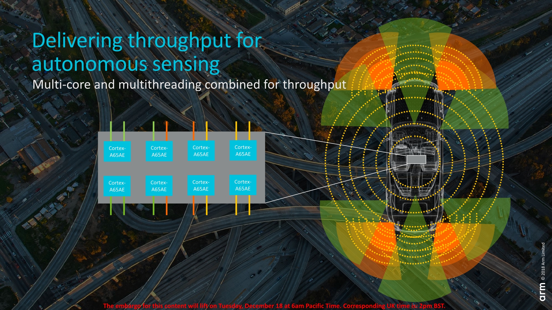
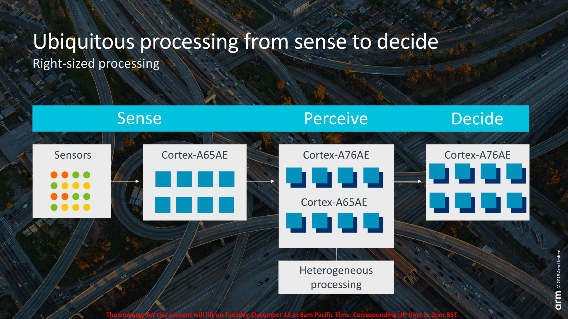
In a practical example of an envisioned system, we would see different clusters of Cortex cores dedicated to different workload tasks. In the above diagram, we would see multiple Cortex A65AE cores in a cluster operate independently in “Split” mode, maximising their throughput when working on sensor data collection.
The data processing would then be passed on to different clusters for perception and decision tasks: Here the cores would require higher levels of functional safety, and thus the CPU cores would be operating in lock-step mode. Arm also emphasised its flexibility in terms of the configuration of the Split-Lock layout of the hardware; it’s something that would be determined on a firmware level, and vendors would be able to reconfigure with a software update if they so wished.
The Cortex A65AE is Arm’s second dedicated core meant for the automotive market - beyond the key aspect that this is an ASIL D compliant microarchitecture, the most interesting aspect of today’s announcement is the fact that it is a new microarchitecture that we yet to see in Arm’s traditional mobile and embedded markets. It seems very much a derivative of Arm’s Cambridge line-up of small CPU cores, and today’s presentation does position the core as the more “traditional little core" alongside the bigger Cortex A76AE.
The Cortex A65AE also Arm’s first SMT core, which is undoubtedly going to generate some talk among our readers. My view on this still unchanged - SMT doesn’t make much sense in mobile workloads as the key focus in this market is energy efficiency. From an electrical engineering perspective, an SMT core will never be more efficient than simply spreading out workloads across more physical cores and clock gating functional blocks when they are being underutilised.
Arm first let it slip that it was planning on introducing SMT during its Neoverse infrastructure IP announcement: Here SMT makes significantly more sense as the workloads and throughput requirements would be very different. If there will be a traditional “Cortex-A65” non-AE variant of this core, it will be very interesting to see how Arm is going to position this, and what markets it will be targeted at. For now, we’ll have to remain patient until further disclosures of the microarchitecture.
Arm envisions first silicon products with the Cortex A65AE in 2020.
Related Reading:
- Arm Unveils Arm Safety Ready Initiative, Cortex-A76AE Processor
- Arm Delivers on Cortex A76 Promises: What it Means for 2019 Devices
- Arm Announces Neoverse Infrastructure IP Branding & Future Roadmap
- Arm's Cortex-A76 CPU Unveiled: Taking Aim at the Top for 7nm
- Arm Unveils Client CPU Performance Roadmap Through 2020 - Taking Intel Head On
- Arm and Samsung Extend Artisan POP IP Collaboration to 7LPP and 5LPE Nodes
- Hot Chips 2018: Arm's Machine Learning Core Live Blog


9 Comments
View All Comments
o4391396@nwytg.net - Tuesday, December 18, 2018 - link
What about ECC memory for automotive devices even for registers as well as ram in these devices (perhaps elsewhere as well) to help against memory induced errors?Wilco1 - Tuesday, December 18, 2018 - link
This is ASIL D, and that requires much more than just DRAM with ECC. See eg. https://www.arm.com/files/pdf/20160628_B02_ATF_Kor...o4391396@nwytg.net - Tuesday, December 18, 2018 - link
Thanks for the write up :)drexnx - Tuesday, December 18, 2018 - link
I wonder what level of functional safety they're taking credit for due to this "compared results" in the same processor approach.typically SIL or ASIL components using redundancy for reduction of probability of dangerous failure would use two (or more) separate processors entirely, not just two threads in the same processor. not entirely sure where they think the risk reduction occurs honestly...
Jorgp2 - Tuesday, December 18, 2018 - link
Did they implement SMT to help fill a wider core?blu42 - Friday, December 21, 2018 - link
Likely. SMT is used to eliminate pipeline bubbles and thus improve the IPC of a pipeline. If CA65 is meant to be a throughput core, then SMT makes sense, as you've guessed it, to better utilize the width of the pipeline. A related reason would be to address codes dominated by high-latency, pipelined ALU ops -- again, by improving throughput. Also, I disagree with Andrei here: an SMTxN pipeline could be more power-efficient than Nx non-SMT pipelines, depending on the workload. That would mean that the factor by which the single SMT pipeline would be slower than the Nx non-SMT pipelines would be less than the factor by which the latter use up more energy than the former.ScouserLes - Saturday, December 29, 2018 - link
Sensors, like all input devices, are generally treated as privileged hardware. Applications software does not have direct access to them. ARM has implemented SMT in a way that allows the two threads to be at different "Exception" (privilege) levels.Without SMT, the 64 bit ARM would have to push a bunch of registers onto the stack, access the sensor and store the value somewhere, then restore the registers. With SMT, one thread (and the registers associated with it) can be be reserved for accessing sensors.
In real time use, sensors are monitored at strictly regular intervals, normally under interrupt. The 32 bit ARM mode has a shadow set of registers for "Fast Interrupt Requests" (FIQ). This is not available in 64 bit mode, but the SMT scheme can emulate - with about 5 times as much register space available.
ARM could have simply extended the FIQ concept to the 64 bit mode, but by adding SMT, they gain a lot of flexibility. As blu42 points out, there are some workloads where SMT can be more power efficient.
ltcommanderdata - Wednesday, December 19, 2018 - link
I wonder how well protected ARM's SMT implementation is from Spectre-like vulnerabilities? If their SMT is only used in lock-step to check for discrepancies instead of independently presumably this isn't a concern.shervinemami - Tuesday, March 8, 2022 - link
According to the official A65 TRM: "The Cortex-A65 core implements the PSTATE SSBS (Speculative Store Bypass Safe) bit that supports software mitigation for Spectre Variant 4 introduced in the Armv8.5-A extension."(https://developer.arm.com/documentation/100439/010...