JEDEC Updates HBM Spec to Boost Capacity & Performance: 24 GB, 307 GB/s Per Stack
by Anton Shilov on December 19, 2018 6:15 PM EST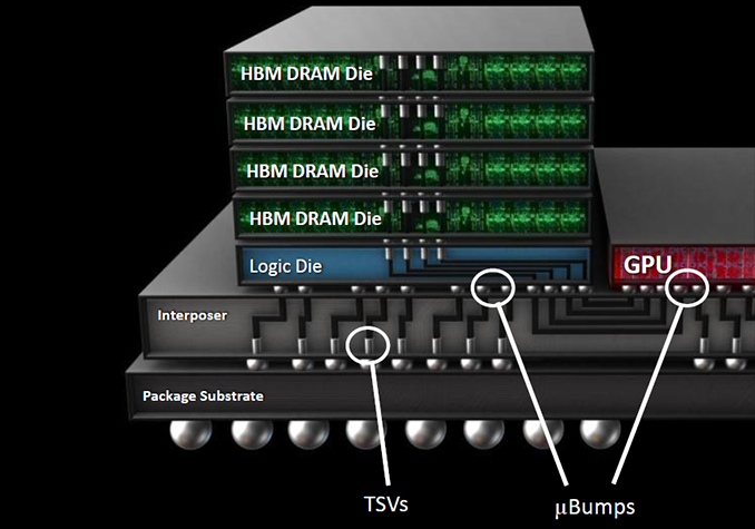
JEDEC this week published an updated version of its JESD235 specification, which describes HBM and HBM2 DRAM. The new version of the standard allows memory manufacturers to increase capacities of future HBM stacks to 24 GB and boost their bandwidth to 307 GB/s per stack.
On the capacity front, the new version of the specification, JESD235B, had added support for 12-Hi chip stacks. With 4 more layers than the previous limit of 8-Hi stacks, this will allow memory manufacturers to produce 12 GB stacks at current densities, and 24 GB stacks in the future when 16 Gb layers become available. Though it's worth noting that while 12-Hi stacks are now part of the HBM specification, the group still lists the physical dimensions of a 12-Hi KGSD (known good stacked die) as "TBD", so it's not immediately clear right now whether 12-Hi stacks will follow the same 720μm typical/745μm maximum stack height rules as the current 2/4/8-Hi configurations. Otherwise the configuration of the stacks themselves are unchanged; the new KGSDs will continue to feature up to eight 128-bit channels as well as a 1024-bit physical interface.
As for performance, the HBM standard now also supports data transfer rates of up to 2.4 Gbps per pin (i.e., 307 GB/s per stack), up from 2 Gbps supported by the JESD235A. It is noteworthy that Samsung’s Aquabolt and SK Hynix’s HBM2 memory chips already support 2.4 Gbps speeds at 1.2 V, so from actual performance point of view the new spec does not bring any significant changes. However this update does finally canonize the 2.4 Gbps data rate into the official standard, and meanwhile the new spec will enable other DRAM makers to release 2.4 Gbps products as well.
All told, the updated specification means that a fully built-out 4096-bit HBM memory subsystem following the JESD235B spec can now contain 96 GB of memory with a peak bandwidth of 1.228 TB/s.
Though it remains to be seen when makers of memory will be ready with their 12-Hi HBM memory chips. To date, no one has announced any 12-Hi products; however I wouldn't expect JEDEC to be adding even taller stacks to the standard unless someone was in the process of building said memory.
Related Reading:
- Samsung Starts Production of HBM2 “Aquabolt” Memory: 8 GB, 2.4 Gbps
- JEDEC Publishes HBM2 Specification as Samsung Begins Mass Production of Chips
- SK Hynix Adds HBM2 to Catalog: 4 GB Stacks Set to Be Available in Q3
Source: JEDEC


15 Comments
View All Comments
ravisurdhar - Wednesday, December 19, 2018 - link
"JEDEC this week published an updated version of its JESD235 specification, which that"*Let me guess, this is by Anton?*
"by Anton Shilov"
*facepalm* Great articles, but get this man an editor.
nandnandnand - Wednesday, December 19, 2018 - link
Anton Shilov is R*ssian (I hope). He needs an editor to check on every article. And I will apply for that job.However, he does cover some of the best topics, even if almost nobody finds 12-Hi HBM s*xy.
p1esk - Thursday, December 20, 2018 - link
I find 96GB HBM sexy...Ryan Smith - Thursday, December 20, 2018 - link
"*facepalm* Great articles, but get this man an editor."Actually he has an editor, who is sheepishly at fault for that typo. I rephrased that sentence and forgot to excise the "that". So it's entirely my own doing...
boeush - Thursday, December 20, 2018 - link
Someone get this editor a grammar-checking tool, pronto! (It's not like MS Word, for instance, has had grammar-checking since, like, 20 years ago...)SeleniumGlow - Friday, December 21, 2018 - link
I recommend Grammarly. It is a system hog, but for content writers, it is a very good tool. It can do contextual checks based on already written sentences too. But I'm sure this comment will get flagged as an advertisement rather than a recommendation.nandnandnand - Wednesday, December 19, 2018 - link
So when Samsung, Rambus, or whoever talk about 3rd generation HBM, is that just marketing hype or prognostication? At what point do we increment to HBM3 or HBM4?I assume we will see 16, 24, and 32-Hi stacks within the next 5 years. What is the limit? Can we see 1024-Hi? That's assuming some good post-NAND technology (not 3D XPoint) doesn't come in and wipe the floor with HBM in the meantime.
Yojimbo - Wednesday, December 19, 2018 - link
HBM 3 is a different specification. I guess they are still researching it and a standard has not yet been finalized. So it's neither marketing hype nor prognostication, but rather future plans in the works. As for when it will come around, I have no idea.Persistent memory technologies tend to be slower than DRAM. The point of HBM is to provide something higher performance than standard DRAM. The part of the market served by HBM will seek to get faster and faster while there is also a separate demand for large capacity, persistent memory with higher performance than NAND. If one technology comes along and fulfills both needs it would be a very strong technology.
Alexvrb - Wednesday, December 19, 2018 - link
Even the best post-NAND tech on the map is maybe within spitting distance of current-gen DDR. Maybe. But GDDR and HBM are another matter entirely, I don't think post-NAND NVRAM is going to be a major threat to volatile graphics memory tech any time soon.vFunct - Thursday, December 20, 2018 - link
Intel/AMD really need to start selling CPUs with HBM as part of the package, to be used as main memory. 96GB is plenty for the vast majority of the people.For server applications that need even more memory, they could sell CPUs that use HBM as L4 cache..