TSMC Reveals 6 nm Process Technology: 7 nm with Higher Transistor Density
by Anton Shilov on April 17, 2019 9:00 AM EST- Posted in
- Semiconductors
- EUV
- TSMC
- 6nm
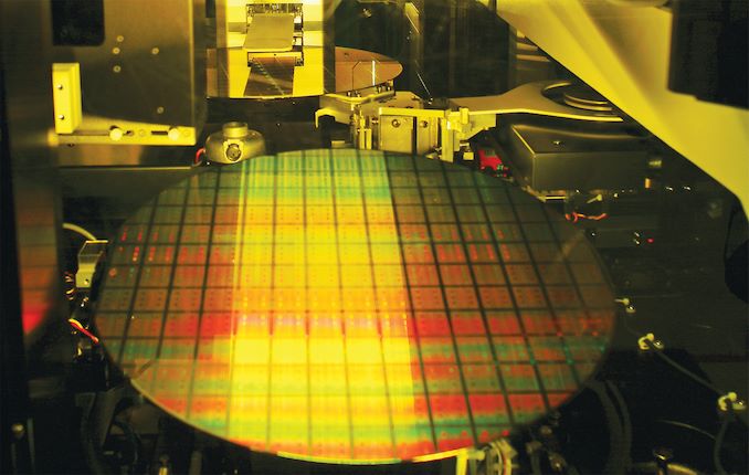
TSMC this week unveiled its new 6 nm (CLN6FF, N6) manufacturing technology, which is set to deliver a considerably higher transistor density when compared to the company's 7 nm (CLN7FF, N7) fabrication process. An evolution of TSMC's 7nm node, N6 will continue to use the same design rules, making it easier for companies to get started on the new process. The technology will be used for risk production of chips starting Q1 2020.
TSMC states that their N6 fabrication technology offers 18% higher logic density when compared to the company’s N7 process (1st Gen 7 nm, DUV-only), yet offers the same performance and power consumption. Furthermore, according to TSMC N6 'leverages new capabilities in extreme ultraviolet lithography (EUVL)' gained from N7+, but does not disclose how exactly it uses EUV for the particular technology. Meanwhile, N6 uses the same design rules as N7 and enables developers of chips to re-use the same design ecosystem (e.g., tools, etc.), which will enable them to lower development costs. Essentially, N6 allows to shrink die sizes of designs developed using N7 design rules by around 15% while using the familiar IP for additional cost savings.
| Advertised PPA Improvements of New Process Technologies Data announced by companies during conference calls, press briefings and in press releases |
|||||||||
| TSMC | |||||||||
| 16FF+ vs 20SOC |
10FF vs 16FF+ |
7FF vs 16FF+ |
7FF vs 10FF |
7FF+ vs 7FF |
6FF vs 7FF |
5FF vs 7FF |
|||
| Power | 60% | 40% | 60% | <40% | 10% | ? | 20% | ||
| Performance | 40% | 20% | 30% | ? | same (?) | ? | 15% | ||
| Area Reduction | none | >50% | 70% | >37% | ~17% | ~15% | 45% | ||
TSMC says that it expects N6 to be used for a variety of applications, including mobile SoCs, GPUs, high-performance computing chips, networking, 5G infrastructure, and other products. What remains to be seen is whether chip designers will be inclined to use N6 technology given its miniscule improvements over N7 when it comes to power, performance, and area (PPA). Perhaps, companies with complex N7-based chips will prefer to go directly to N7+, or even 5 nm (CLN5FF, N5), for their next generation parts.
TSMC will start risk production of chips using its N6 fabrication technology in the first quarter of 2020. Keeping in mind that it usually takes companies about a year to start high-volume manufacturing (HVM) after the beginning of risk production, expect N6 to be used for mass products starting from 2021.
Related Reading:
- TSMC’s 5nm EUV Making Progress: PDK, DRM, EDA Tools, 3rd Party IP Ready
- TSMC: 7nm Now Biggest Share of Revenue
- TSMC: First 7nm EUV Chips Taped Out, 5nm Risk Production in Q2 2019
- TSMC Details 5 nm Process Tech: Aggressive Scaling, But Thin Power and Performance Gains
Source: TSMC


23 Comments
View All Comments
MananDedhia - Wednesday, April 17, 2019 - link
This is a marketing release - since they are not revealing the 2 painfully obvious points of improvement - what is the minimum fin pitch and is EUV inserted at MOL or only BEOL? The improvement in the process is re-assuring and TSMC does have a good track record of executing on its timelines. Lets see where this goes.ZolaIII - Wednesday, April 17, 2019 - link
Lol it's a same old 7 nm utilising denser rooting libs.name99 - Thursday, April 18, 2019 - link
How many times do I have to repeat this?You simply don't understand the foundry business model!
TSMC does not sell one leading edge process and done! They sell a variety of processes, and part of the sale includes continual upgrades of the non-leading edge processes, so that even if you don't have the budget to fully redesign and run a new mask set for the newest process, you may be able to get some improvement (slightly denser, or lower power, or faster) with the much smaller modifications required to move from say 7nm to 7nm+ or 6nm.
Just because these sorts of improvements (like ongoing improvements at 10 or 16, or even 28nm) are not of interest to, say, Apple, doesn't mean they're of no interest to anyone...
Santoval - Wednesday, April 17, 2019 - link
Will this become available before or after TSMC's N7+? The article appears to suggest that N6 will be released after N7+ ("..companies with complex N7-based chips will prefer to go directly to N7+..), however the table listing the various nodes appears to suggest the opposite.In any case, N6 looks like it will be identical to N7+ in transistor density gain, so for all intents and purposes it just might the same node.
Santoval - Wednesday, April 17, 2019 - link
edit : I rather meant that "The article appears to suggest that N7+ will be released after N6..."Frenetic Pony - Wednesday, April 17, 2019 - link
This appears to be released over concern about initial usage of N7+. From the wording it seems 7+ chips aren't actually compatible with N7 designs, meaning companies would have to redesign their chips all over again to get relatively little power and density gains, while they wouldn't have to with N6.No doubt Apple can afford N7+ designs and it'll show up in the next iPhone. N6 is probably meant for AMD and other companies that don't see the benefit to spending hundreds of millions for little improvement. So we might see a Navi refresh, and the PS5, and whatever on N6 next year.
brakdoo - Wednesday, April 17, 2019 - link
You're so weird: This is a rebrand of N7+ at lower cost with very little difference. Just watch the earnings call tomorrow...FreckledTrout - Wednesday, April 17, 2019 - link
Anton, how does this compare to Intel's 10nm and 7nm? Personally I think TSMC's choice of taking small steps is the right one going forward as the incremental changes are less risky. However there naming schemes of processes seem a bit overly optimistic in fact I would go as far is it's mostly marketing.peevee - Thursday, April 18, 2019 - link
" Intel's 10nm and 7nm"What Intel's 10nm and 7nm?
Roland00Address - Thursday, April 18, 2019 - link
It is less risky but you have to realize the inputs to understand the outputs of why TSMC took this strategy and the associated strategy benefits and strategy downsides plus the strategy's credits and the strategy's tax.TSMC has multiple customers and the first customer for the process (to test the process) are using both smaller chips and "known chips." It is easier to have multiple process running in the company and still be at full capacity and there is cheaper development for you needed to have all these different designs for you are foundry that other people bring their chips to instead of using the foundry for only internal use.
Intel by contrast has a lot less amount of designs in play, various chips for server, desktop, laptop, and mobile / modem (and the mobile / modems are being phased out.) Plus chips that run on older processes. This has its pros and cons for it is easier to tailor the maximum performance for these chips via process changes if you can actually get the process right, but if you have problems getting the process right TSMC choice of many designs and just make sure your fabs are at full capacity makes sense for it is easier to iterate to the next step in the process.
My point here is I think TSMC is doing the smarter thing style of strategy, but there is a reason why Intel is doing the strategies they have been doing, and it is not like overnight Intel could adopt TSMC strategies for the inputs are not there with lots of foundry customers to get the desired output of a specific style of strategy.