AMD Clarifies Comments on 7nm / 7nm+ for Future Products: EUV Not Specified
by Dr. Ian Cutress on March 5, 2020 6:50 PM EST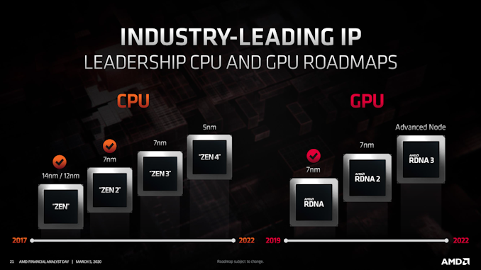
As part of AMD’s Financial Analyst Day 2020, the company gave the latest updates for its CPU and GPU roadmap. A lot of this we have seen before, with the company talking out to Zen 4 and Genoa on its datacenter CPU product line, out to Zen 3 and Ryzen 4000 with the consumer product line, and now with the RDNA/CDNA split between consumer and compute graphics. In previous graphs of a similar nature, AMD used the term ‘7nm+’ when referring to products beyond the first iteration of 7nm. AMD has today clarified to us that this does not mean they are using TSMC’s N7+ process node for those items.
TSMC has three high-level versions of its 7nm process:
- N7, which is the basic initial version using ‘DUV’ only tools (so no EUV),
- N7P, which is the second generation version of N7 which is also only DUV
- N7+, which is an EUV version of N7 for a number of layers in the metal stack
This nomenclature has been finalized within the past year or so.
Before this, AMD had presented various CPU and GPU roadmaps to the public. For the Zen 2 hardware, such as Ryzen 3000 series (Matisse), AMD had labeled this as ‘7nm’, which was all widely interpreted to mean TSMC’s N7 process. For future products, such as Zen 3, AMD had the slide listed as ‘7nm+’, which everyone had understood was ‘a better version of 7nm’.

Example Roadmap from CES 2018
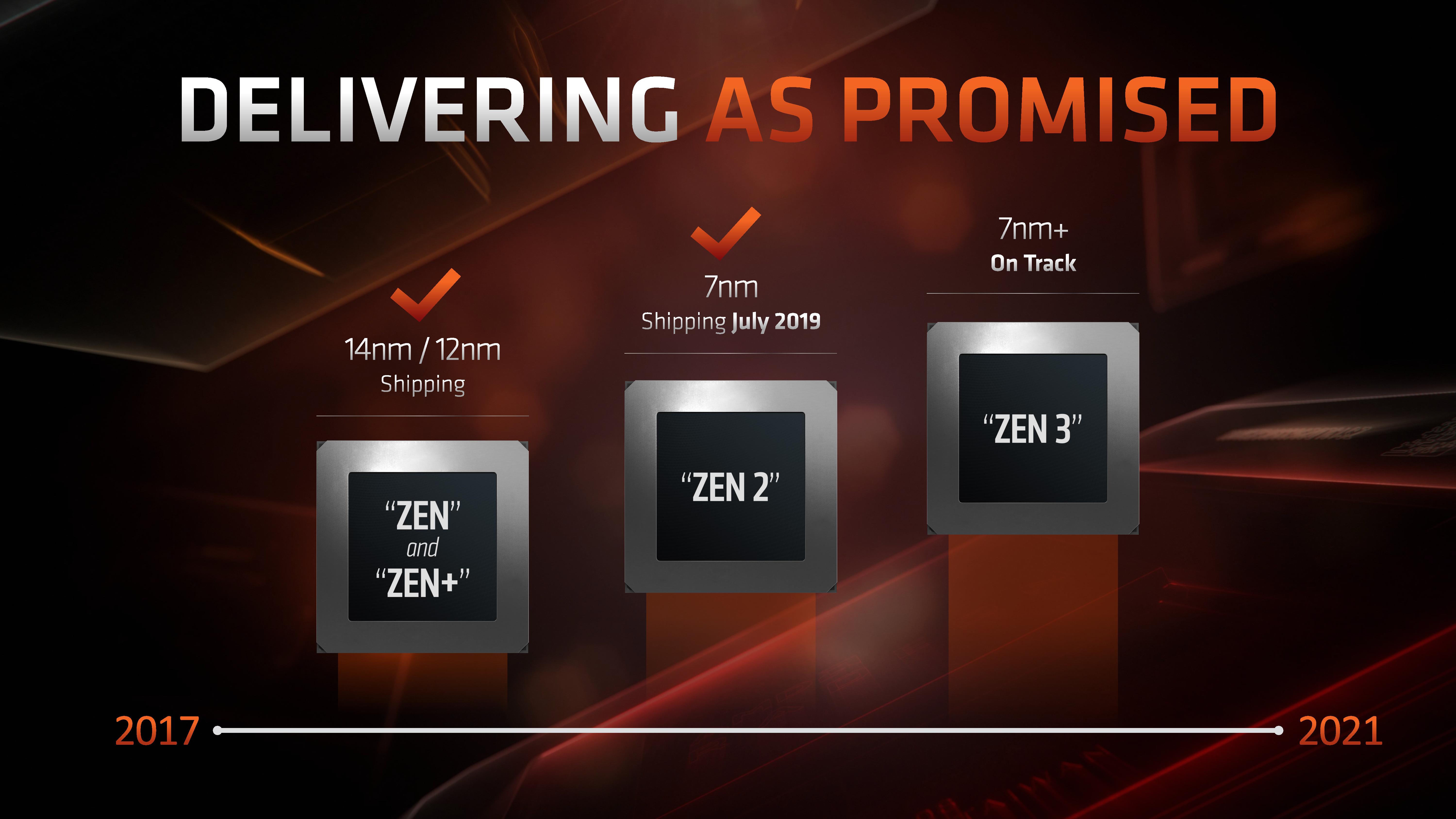
From Next Horizons in July 2019
Because AMD labeled those as 7nm+, when TSMC called its version of 7nm with EUV to be N7+, one of the obvious assumptions that people have made is that where AMD wrote 7nm+, it was to be on the N7+ process. We have since learned that this is not entirely correct.
In order to avoid confusion, AMD is dropping the ‘+’ from its roadmaps. In speaking with AMD, the company confirmed that its next generations of 7nm products are likely to use process enhancements and the best high-performance libraries for the target market, however it is not explicity stating whether this would be N7P or N7+, just that it will be ‘better’ than the base N7 used in its first 7nm line.
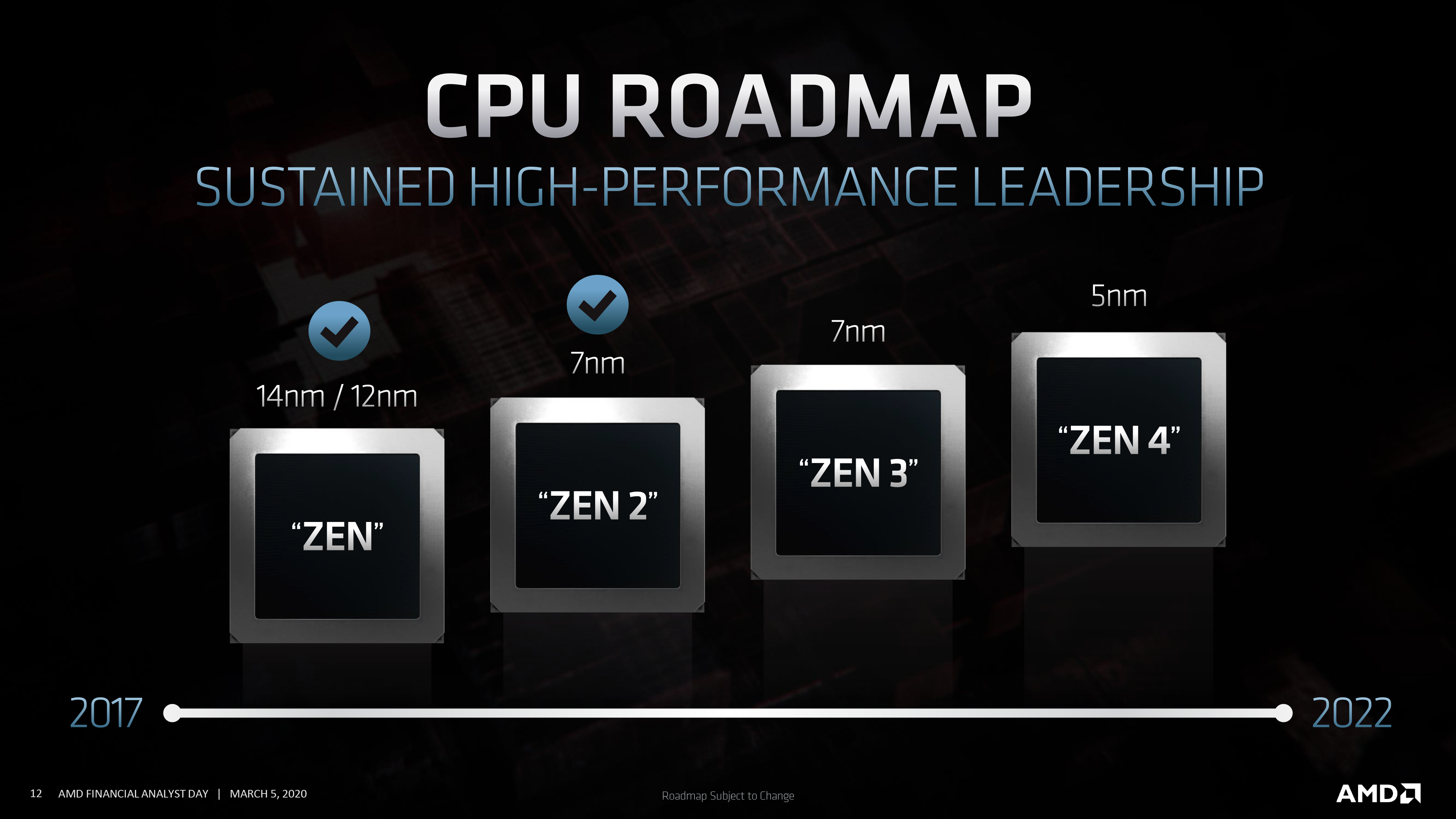
This doesn’t necessarily mean that AMD isn’t going to be using EUV in the future – we were told it will be on a case by case basis, and at this time they wanted to clarify that AMD is not making any specific clarifications of which version of 7nm from TSMC it plans to use. More will be detailed at future events.
Interested in more of our AMD Financial Analyst Day 2020 Coverage? Click here.


37 Comments
View All Comments
ToTTenTranz - Thursday, March 5, 2020 - link
Aren't most long-living N7 products supposed to become N6 anyway?dotjaz - Thursday, March 5, 2020 - link
But AMD never used vanilla N7extide - Friday, March 6, 2020 - link
Um, yes it did. It even says so in the article:"however it is not explicity stating whether this would be N7P or N7+, just that it will be ‘better’ than the base N7 used in its first 7nm line."
"base N7 used in its first 7nm line"
Vega 20 must use it, and I believe the Zen2 CCDs do as well.
dotjaz - Friday, March 6, 2020 - link
Nope vailla N7 has M1/BEOL scale of 1.0x and 13 metal layers, AMD used 1.45x and 14 layers, that's why AMD's N7 "Large Die" had half the density. Their GPU is even worse in term of density, they used 7.5T instead of 6T.So in summary compared to base N7, AMD's version has different gate/metal size, more metal layers, allows different track count, if you call that "vanilla" I don't know what's not "vanilla".
FreckledTrout - Monday, July 13, 2020 - link
AMD never used/uses the initial new node from TSMC because those are always for low power ie iPhone chips etc. TSMC takes about 1 year to tweak said process for high power which you will see some density losses to allow higher frequencies.AnGe85 - Friday, March 6, 2020 - link
For example Vega 20 and Zen2 use N7.dotjaz - Friday, March 6, 2020 - link
No they don't. Zen2 use N7 "Large Die" which had different scale and metal layer count. Vega 20 goes further to use 7.5T library.NONE OF THOSE were offered in N7. Qualcomm used "high performance" N7 lib which only relaxed CPP from 54nm to 57nm
dotjaz - Friday, March 6, 2020 - link
*57nm to 64nmAnGe85 - Saturday, March 7, 2020 - link
You are confusing manufacturing process (N7) with its associated cell libraries (e.g. H240 HD (6T) and H300 HP (7.5T)). Apples A12, A12X, the Kirin 980, Snapdragon 855 and AMDs Vega 20 and Zen 2 all use(d) TSMCs CLN7FF aka N7 process.Additionally density does not directly result from used libraries, instead it depends on the design goals. Vega 20 most likely used H300 HP, but for Zen 2 AMD switched to H240 HD. The Snapdragon 855 uses for the so-called prime core, a single, faster Kryo 485 Gold the H300 HP lib, but for all remaining seven cores and the rest of the SoC the H240 HD lib and still archives a much higher density than AMD with its chiplet, because the design goals have been different.
Avg. MTr/mm2:
Vega 20 = ~ 40
Zen 2 = ~ 52
SD 855 = ~ 91
(To complete the wrap-up, there has also been a high performance H360 HP lib (9T) for the N7, which has become obsolete over time.)
AnGe85 - Friday, March 6, 2020 - link
N7P (DUV only) and N7+ (4 layers EUV) are production-ready since mid 2019.