Intel’s 11th Gen Core Tiger Lake SoC Detailed: SuperFin, Willow Cove and Xe-LP
by Dr. Ian Cutress on August 13, 2020 9:01 AM EST- Posted in
- CPUs
- Intel
- SoCs
- Tiger Lake
- 10+
- Xe-LP
- Willow Cove
- Intel Arch Day 2020
- SuperFin
- 10SF
What is 10nm SuperFin All About?
For those within the semiconductor industry, as well as individuals with investments in the companies we cover, it has been hard to miss the recent news surrounding Intel’s manufacturing process woes. In short, Intel’s 10nm process technology has failed to match expectations in performance and yield, coming in a couple of years later than expected and with an inability to compete with its own previous generation products. It still remains in low volume today, with Tiger Lake expected to be the first true example of what Intel’s vision 10nm was meant to be.
The next step function change in Intel’s manufacturing, the move to 7nm using Extreme Ultra Violet (EUV) technology, has recently been announced that it also has an additional six month delay. With news like this, it has become a struggle to remain confident about Intel’s ability to deliver an industry-leading manufacturing node technology that is competitive in the market. This used to be the position that Intel held until delays crept into the 10nm process.
Intel’s Ruth Brain, Senior Transistor Architect, Covering Intel’s Engineering Feats
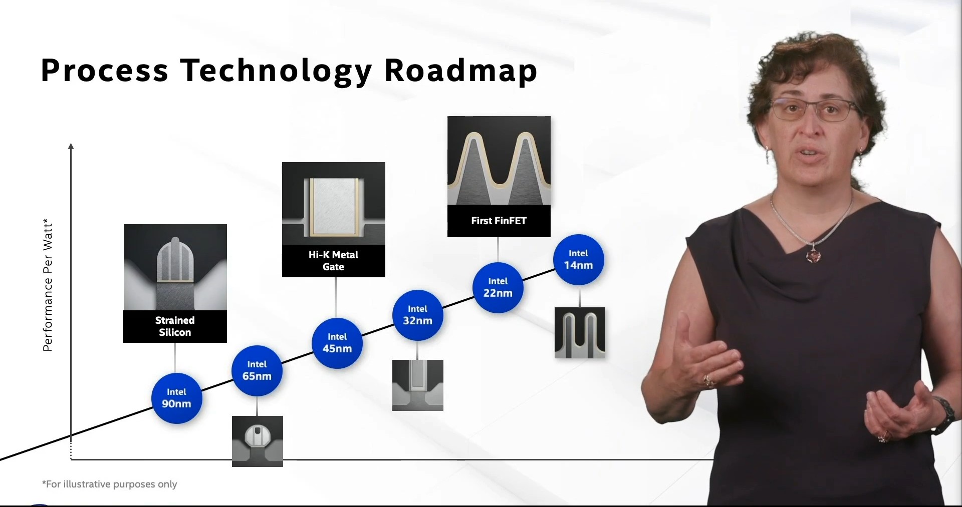
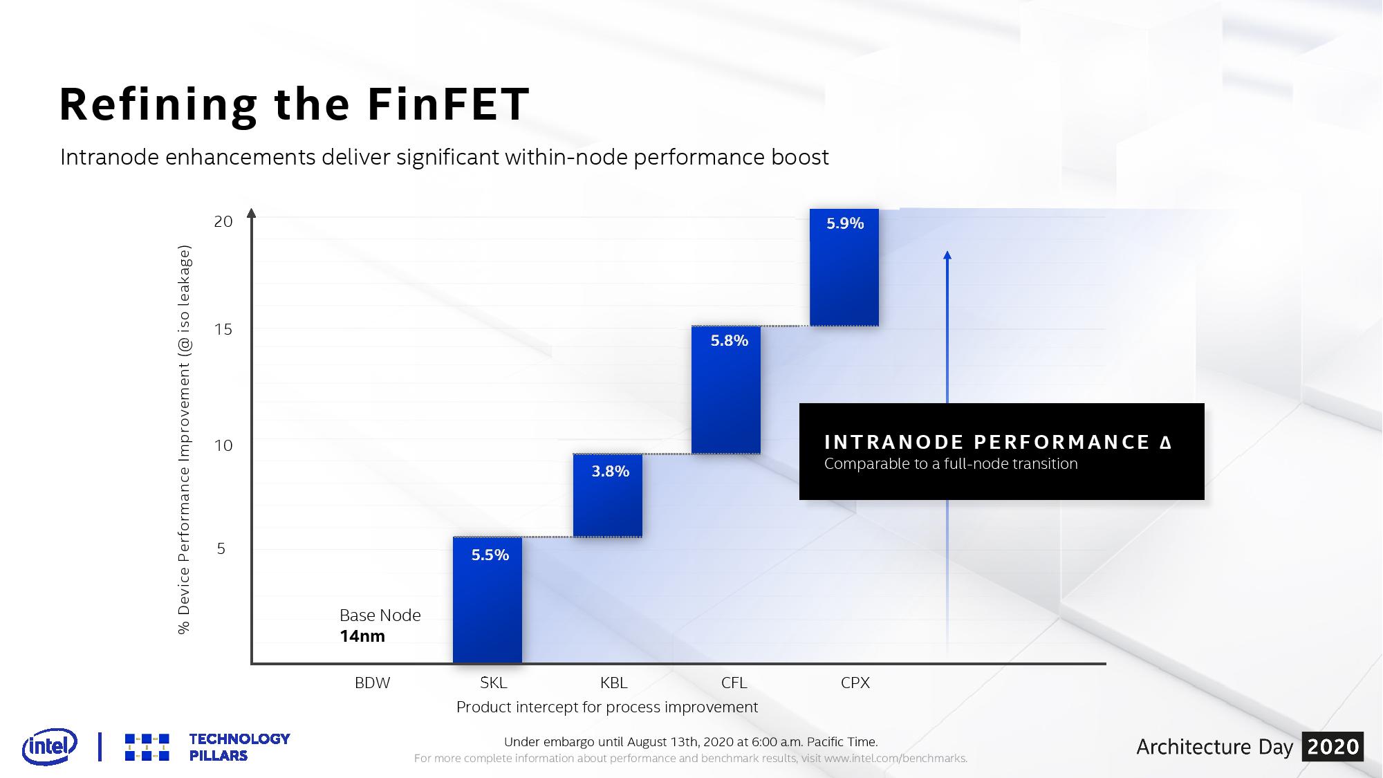
Intel’s disclosures on its manufacturing technology vary in complexity depending on how successful the product is perceived internally. When Intel first announced FinFETs on its 22nm process node, in May 2011, there was a lot of information straight out of the gate, and the node was very successful. With the next generation of 14nm, there were some delays with the initial generation of Broadwell products, but ultimately the process was explained in detail by the company at its own event and we published our article on 14nm in August 2014. The 14nm process node has been Intel’s most profitable manufacturing node to date, and continuous intranode enhancements over the years (14+, 14++, 14+++, 14++++*) have given the company an effective enhancement equivalent to a pure node update within a manufacturing generation.

*Yes, Intel has a 14++++ node. It’s even in their diagrams. The only product confirmed to be on 14++++ as far as we can tell is the Cooper Lake Xeon Scalable family.
When it comes to 10nm, the situation is not as rosy, even compared to the delays on 14nm. To date, Intel has had two generations of 10nm products on the CPU side, one of which the company steers away from even trying to mention it in public, even though we’ve reviewed it in excruciating detail.
Cannon Lake, the first 10nm product, found its way into Intel’s Crimson Canyon NUC mini-PCs and was a hot mess: two cores only, disabled integrated graphics, and although it shipped for revenue in 2017, Intel was right to consign it to history very quickly.
Ice Lake was Intel’s proper launch vehicle for 10nm, offering four cores and a lot of Gen11 graphics within 15 watts. It has found its way into over 50 laptop designs, but as mentioned on the previous page, despite its 15-20% increase in raw performance clock-for-clock, that 10-20% decrease in frequency balances it out for a minimal CPU improvement over 14nm. The graphics on Ice Lake are still a lot better than on 14nm, and support for Thunderbolt 3 as well as 512-bit vector instructions means that Ice Lake still has a few plus points.
As it stands, because Intel doesn’t want to consider Cannon Lake as a true part of its heritage, Ice Lake was deemed a flat ‘10nm’ product, with no plusses and no extra bits. After Ice Lake was set to be Tiger Lake, built on a ‘10+’ manufacturing node.
+, ++, +++, ++++: What is a Name
A side note about manufacturing process naming. As many of our readers are aware, the actual number attached to the process in the era of FinFET technology has effectively become nothing more than a proper noun for the process node technology – it isn’t related to any feature within the products built on that process. It gets especially confusing when there are features of a process built at a smaller scale than the number on the technology: for example, Intel’s 10nm actually has features that are 8nm in size. Manufacturing nodes might as well be given names like Gordon, Eric, or Lisa, in order to stop the confusion that having that number provides.
Within a generation of a process node technology, the company fabricating the semiconductor orders may periodically update its manufacturing process but still keep it, by and large, within the confines of that generation. These updates are often minor, but are called BKM (best-known-method) updates and can lead to simple frequency or power efficiency improvements – perhaps on the order of 50 mV or 25 MHz, but sometimes afford bigger gains.
When we were dealing with planar transistors, at 22nm, 32nm, 45nm and above, these BKM updates were par for the course during the lifecycle of a product built at that node. Improvements in the manufacturing were taken, rolled into the product automatically, and it was simply sold in the same box without much of a fuss, but had marginally better characteristics.
As we’ve moved into multiple generations of FinFET technologies, where creating a leading edge high-performance processor can cost $10-$100million or more, these BKM updates have become marketable updates to both the chip design companies and the fabs they are built on. Small tweaks to the BKM are now being used to launch new waves of products, and offer the companies involved a chance to create column inches and highlight the engineering prowess of the teams involved, as well as offering the customer a better product.
Different fabrication plants have marketed these updates in different ways. Intel has gone with the +,++,+++,++++ nomenclature for its 14nm process, with each step giving better transistor device performance and being rolled into new generations of products:
However, Intel’s naming scheme has become somewhat of a meme and a joke over the past few years. With the company’s inability to bring out 10nm on its initial schedule, Intel decided to add more + to each new process update on 14nm. As 10nm was delayed further, consumers and users saw another + added to 14nm. The meme of Intel unable to get 10nm working and seeing a 14+++++++++ future product is a fundamental strike to the soul of a company that has spent the last 30+ years priding itself on its ability to drive leading edge semiconductor manufacturing for high-performance.
As Intel has slowly moved onto its 10nm product portfolio, the + naming came in again almost immediately. 10nm for Cannon Lake, 10+ for Ice Lake which later became just ‘10nm’, 10+ for Tiger Lake, and then 10++ and 10+++ were all exhibited on roadmaps at various industry events. The same story goes on for future processes, such as 7nm and 5nm.

If it makes you feel any better, Intel’s own engineers said that even they sometimes have difficulty remembering which + variant has specific updates, or which product is built on which + node. Ultimately, while the + serves a purpose, it has ultimately become confusing for customers and engineers alike.
This is why, behind the scenes, we have told Intel that it has to move away from + and ++ and +++, if only from a corporate image standpoint. Where its manufacturing competitors like TSMC and Samsung can point to different variants of their 10nm processes for different products, all Intel has is more pluses.
Other press and analysts have told Intel this too. However, based on previous experiences, we rarely get to speak to the people who actually can cause direct change. All our contacts can do is try, and pass our comments up the chain, hopefully with as much passion as we have. The people that can actually sign off on changes like this are often not very press facing.
But someone, somewhere at Intel, has finally heard our pleas. Today Intel is approaching its 10nm portfolio from a different angle. While nothing is technically changed under the hood, the new strategy allows the company to market its manufacturing and products from an initial context of the deep engineering portfolio and research that occurs. The first result of this change is the SuperFin.
Intel 10SF: The Largest Single Intranode Enhancement in Intel History
10nm SuperFin is what Tiger Lake is built on, and represents the new name for 10+. As part of Intel’s 10SF, we’re getting a glimpse into what makes 10SF different to the 10 for Ice Lake , as well as updates on some key parts to the design of the transistors and metal stack that make up the 10SF process.
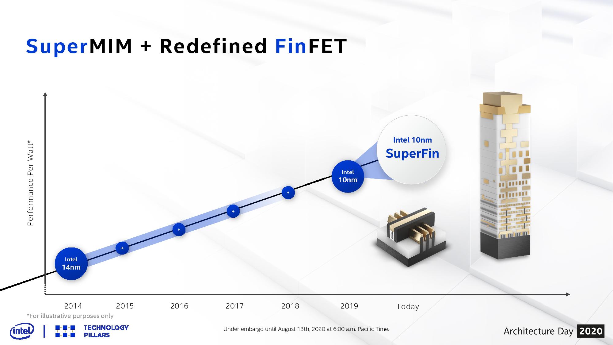
10SF builds on 10nm by introducing a redefined FinFET design (Intel’s 4th Gen FinFET?) with increased Fin performance, as well as a new SuperMIM (metal-insulator-metal) capacitor design.
The updated FinFET design focuses on three areas.

Through new manufacturing techniques, the epitaxial growth of crystal structures on the source and drain has been enhanced, ultimately increasing the strain in order to lower the resistance allowing more current to flow through the channel.
An enhanced source/drain architecture and improved gate manufacturing process helps drive additional higher channel mobility, which enabling charge carriers to move more quickly and improves transistor performance.
Additionally a larger gate pitch to enable higher drive current for certain chip functions that require the most performance. Normally a larger gate pitch sounds the opposite of what we want for a dense process node technology, however it was explained that in this case making the transistor bigger with improved performance actually means that fewer buffers are needed in the high performance cell libraries, and ultimately the cell size decreases as a result. Note that on some of Intel’s 14nm variants, one of the techniques used to help drive higher frequency was a larger gate pitch.
For the metal stack, Intel makes some very bold claims with impressive technology.
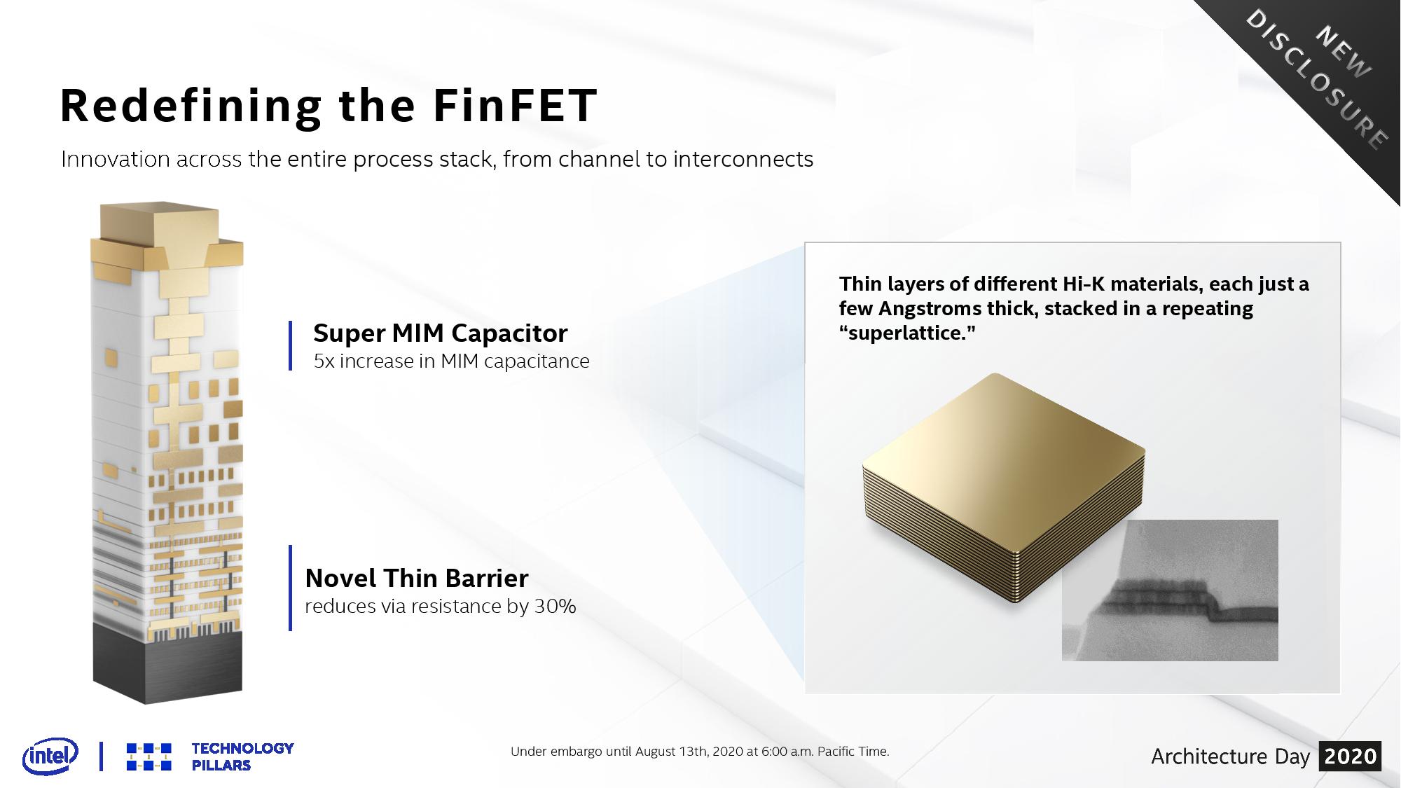
At the lower layers of the stack, Intel is introducing a new set of barrier materials to enable thinner barriers, which also helps reduce resistance of vias by up to 30% by enabling the metal each via to be a bigger proportion of the fixed size. Reducing the resistance enhances the performance of the interconnect between the metal layers
At the higher levels, Intel is introducing a new SuperMIM (metal-insulator-metal) capacitor. Intel states that this new design gives a 5x increase in capacitance over an industry standard MIM cap within the same footprint. This drives a voltage reduction that ultimately leads to drastically improved product and transistor performance. Intel states that this is an industry first/leading design, enabled through careful deposition of new Hi-K materials in thin layers, smaller than 0.1nm, to form a superlattice between two or more material types.
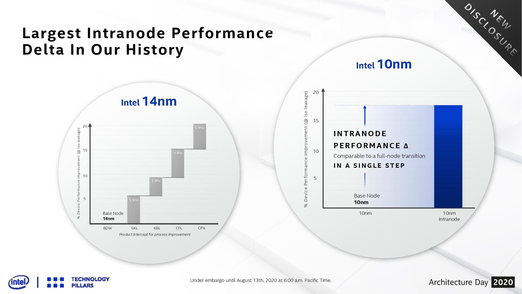
All combined, Intel’s Senior Transistor Architect, Ruth Brain, states that these features enable the ‘Largest single (intra)node enhancement in Intel history’, enabling 17-18% better transistor performance from the base 10nm designs. This makes 10SF equivalent to a full node enhancement over Intel’s base 10nm process. To draw parallels to Intel’s 14nm, 10SF to 10 is the equivalent of Coffee Lake (14+++) to Broadwell (14nm).
Beyond SuperFin to Enhanced SuperFin
As part of Architecture Day 2020, Intel also stated that the intranode update beyond 10SF will be called 10ESF, or 10 Enhanced SuperFin. No specific details were given as to what 10ESF will provide over 10SF, only that it will bring additional performance and interconnect innovations.
That being said, Intel stated that it would be optimized for the datacenter, which likely means that some characteristics will be changed in order to support the increased thermal and current density that comes with vector acceleration. Intel, perhaps accidentally, confirmed to us that there will be three products based on 10ESF.
| Products using Intel 10SF and 10ESF | |
| 10SF | Tiger Lake Xe-LP (SG1, DG1) Xe-HPC Ponte Vecchio Active Interposer Tile |
| 10SFE | Xe-HP Xe-HPC Ponte Vecchio Rambo Cache Tile Sapphire Rapids |
(Intel has stated that Ponte Vecchio will have four types of tile: base, compute, Rambo Cache, and Xe Link. The others not mentioned will be split between 7nm and external fabs. More on that info in a separate article)


71 Comments
View All Comments
Quantumz0d - Thursday, August 13, 2020 - link
"The others not mentioned will be split between 7nm and external fabs. More on that info in a separate article"So that means they are going for external fab really. Damn. What a shame. I wonder if that's the CPU or this GPU. Anything is a shame on Intel and that beancounter Bob.
IanCutress - Thursday, August 13, 2020 - link
That's referring to the other tiles of Ponte Vecchio. There are 4. We covered 2.Eliadbu - Thursday, August 13, 2020 - link
Shame is when you don't acknowledge your problems and how they might limit you. Going with external fabs allows the company to be competitive where it needs the most. But they sure need a long term strategy and and make critical decisions like which processes they would utilize earlier.Kangal - Thursday, August 13, 2020 - link
It's only GPU.And it's only the Xe-HP (ergo Discreet GPU) variant.
It seems to imply that is only on the 10SFE "enhanced" variant. Basically using TSMC 7nm process for the higher memory and connector chips, named as "Rambo Cache" and "Xe Link". And that's targeting the server market and high-end desktops (ie think Nvidia Titan).
Seems like Intel realise how embarrassing it is to ask for their competitors wafers for their main product, so instead they're taking a half-measure and using it for the GPU only. That way they get to save face and say "well, AMD and Nvidia do it too". Also it seems they couldn't get any good prices, which is why only some chips are made on the 7nm, and rest are made in-house on 10nm. Overall, this is Intel playing hard to catch up to TSMC's 7nm and AMD's Zen2 and AMD's Vega. That's why the whole thing is difficult to understand, as it is purposely obfuscated. Yet these will only ship in (late) 2021, whereas the competition is posied to actually leap ahead in 2020 to +7nm TSMC, Zen3, RDNA2. And when Intel arrives, they might even be facing off against 5nm and a Zen3+ refresh. Just to put things into perspective.
tipoo - Thursday, August 13, 2020 - link
This reads quite promising. Great writeup."A few angstroms thick" it's hard to even think about the scale of this stuff, that's 0.1 nanometres or 100 picometres. How far from atomic bonding limits?
DrJackMiller - Thursday, August 13, 2020 - link
It's pretty damn close, but that depends on the bond :-). For a perhaps more human comparison, that of O-O in Oxygen is 1.208 Å; and in C=O bonds (e.g. in CO2) it's around 1.16 Å.vortmax2 - Friday, August 14, 2020 - link
Would love to see an article here of the next 10-20 years of processors as we enter deeper into the atomic scale. What the next big breakthrough?jospoortvliet - Saturday, August 15, 2020 - link
Less promising is that they went for a four cores design again. With AMD pushing the desktop to 8 with the first Zen you would think they would realize amd would pull the same when going mobile and prepare for it... so is this arrogance thinking their cores are so much better or they control the market? Lack of strategic insight? Or inability to work out things for the yield and cost math?Spunjji - Monday, August 17, 2020 - link
If these cores are as good as they're claiming they are, there will be a legitimate dilemma choosing between 4 Very Fast cores and 8 Really Quite Fast cores.I'd wager that yields are 80% to blame and power is the rest - they have an 8-core Tiger in the works, but it's a 35/45W part and there's nothing firm about a release date yet.
none12345 - Tuesday, August 18, 2020 - link
Depends on the atoms, but for reference how about silicon."Silicon has the diamond cubic crystal structure with a lattice parameter of 0.543 nm. The nearest neighbor distance is 0.235 nm."
Diatomic hydrogen is the smallest molecule with a bond length of 0.74 angstrom.
Bond length is typically 1-2 angstrom.
"Intel states that this is an industry first/leading design, enabled through careful deposition of new Hi-K materials in thin layers, smaller than 0.1nm, to form a superlattice between two or more material types."
Unless im missing something, the above statement does not make any sense to me. thin layers of atoms less then the average bond length between atoms is nonsensical.