Intel Updates Data Center Roadmap: Xeons On Track - Emerald in Q4'23, Sierra Forest in H1'24
by Ryan Smith on March 29, 2023 11:30 AM EST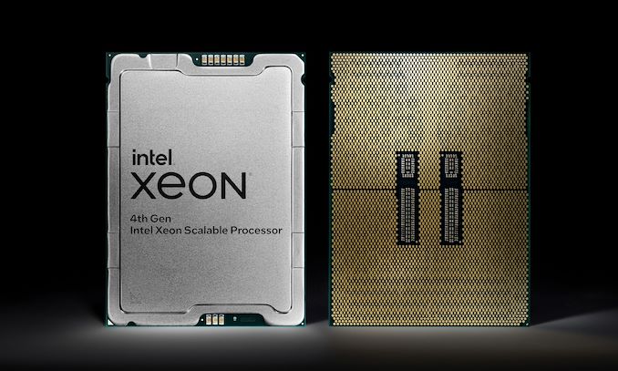
Coming to the end of the first quarter of 2023, Intel’s Data Center and AI group is finding itself at an interesting inflection point – for reasons both good and bad. After repeated delays, Intel is finally shipping their Sapphire Rapids CPUs in high volumes this quarter as part of the 4th Generation Xeon Scalable lineup, all the while its successors are coming up very quickly. On the other hand, the GPU side of the business has hit a rough spot, with the unexpected cancelation of Rialto Bridge – what would have been Intel’s next Data Center GPU Max product. It hasn’t all been good news in the past few months for Intel’s beleaguered data center group, but it’s not all bad news, either.
It’s been just over a year since Intel last delivered a wholesale update on its DCAI product roadmaps, which were last refreshed at their 2022 investors meeting. So, given the sheer importance of the high margin group, as well as everything that has been going on in the past year – and will be going on over the next year – Intel is holding an investor webinar today to update investors (and the public at large) at the state of its DCAI product lineups. The event is being treated as a chance to recap what Intel has accomplished over recent months, as well as to lay out an updated roadmap for the DCAI group covering the next couple of years.
The high-level message Intel is looking to project is that the company is finally turning a corner in their critical data center business segment after some notable stumbles in 2021/2022. In the CPU space, despite the repeated Sapphire Rapids delays, Intel’s successive CPU projects remain on track, including their first all E-core Xeon Scalable processor. Meanwhile Intel’s FPGA and dedicated AI silicon (Gaudi) are similarly coming along, with new products hitting the market this year while others are taping-in.

Sapphire Rapids: 4th Generation Xeon Scalable Shipping in Volume
Following what can only be described as a prolonged development process for Intel’s next generation Xeon Scalable processors, Sapphire Rapids finally began shipping in volume over the past few months. The Q1’23 (ed: or is that Q5’22?) launch of the product has come later than Intel would have ever liked, but the company is finally able to put the development process behind them and enjoy the fruits of shipping the massive chips in high volumes.
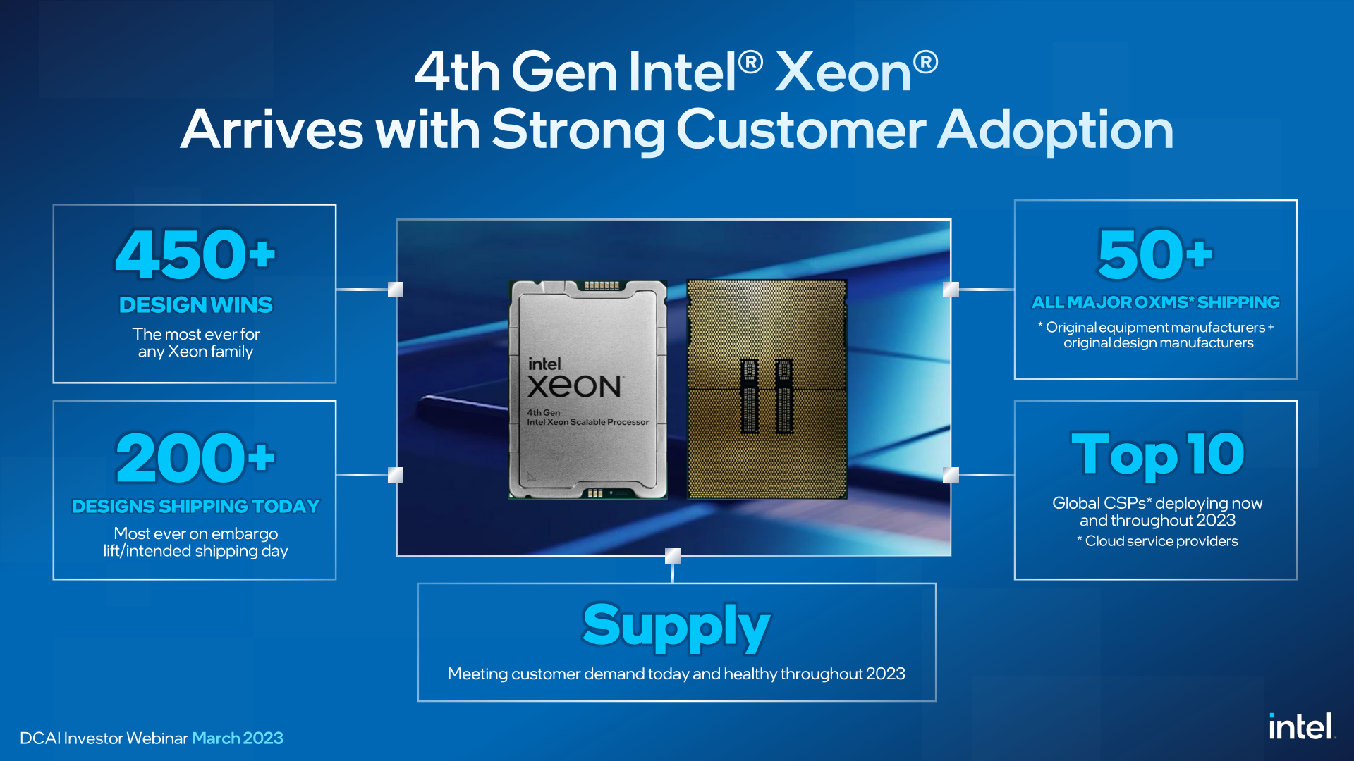
At this point Intel isn’t quoting precise shipment numbers – back at launch, the company said it expected to make it to a million units in record time – but the company is doubling-down on their claims that they’ll be able to product the large, complex chips in high enough volumes to meet customer demand. Built on the Intel 7 process, the final iteration of what started as Intel’s 10nm line, Intel is benefitting from that well-tuned process. At the same time, however, the 4th Generation Xeon Scalable lineup includes Intel’s first chiplet-based Xeon design, so it is still not the easiest launch.
Besides meeting customer demand, Intel’s main point is that all of their major customers are adopting the long-awaited chips. This is largely unsurprising given that Intel still holds the majority of the data center CPU market, but given the investor audience for today’s announcements, it’s also unsurprising to see Intel explicitly calling attention to this. Besides a generational improvement in CPU core architecture, Sapphire Rapids also delivers everything from DDR5 to PCIe 5/CXL support, so there is no shortage of interest in replacing older Ice lake and Cascade Lake (3rd & 2nd Gen Xeon Scalable) hardware with something newer and more efficient.
Intel, of course, is looking to fend off arch-rival AMD from taking even more market share in this space with their EPYC processors, which are now on to their 4th generation (9004 series) Genoa parts. There are a few demos slated to be run this morning showcasing performance comparisons; Intel is keen to show investors that they’re shipping the superior silicon, especially as AMD has the advantage in terms of core counts. So expect Intel to focus on things like their AI accelerator blocks, as well as comparisons that pitch an equal number of Sapphire Rapids (Golden Cove) and Genoa (Zen 4) CPU cores against each other.
Emerald Rapids: On Track for Q4’23, Will Be 5th Generation Xeon Scalable
Diving into the future of Intel’s product roadmap, the first disclosure from today’s event is an update on the status of Emerald Rapids, the architectural successor to Sapphire Rapids. Intel’s previous roadmap had chips based on the architecture slated to arrive in 2023, a launch cycle that has been increasingly called into question given Sapphire Rapids’ delay to 2023. But sure enough, Intel still expects to deliver the next generation of Xeon processors later this year, in Q4.
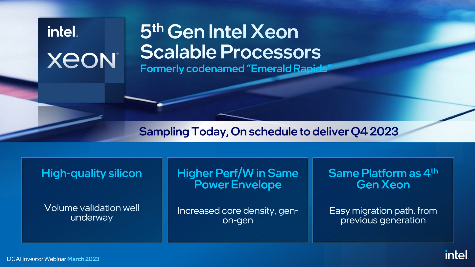
According to Intel, Emerald Rapids chips are already sampling to customers. At the same time, volume validation is already underway as well. As Emerald Rapids is a relatively straightforward successor to Sapphire Rapids, Intel is looking to avoid the long validation period that Sapphire Rapids required, which will be critical for making up for lost time and getting the next Xeon parts out by the end of this year.
Given that this is an investor meeting, Intel isn’t offering much in the way of technical specifications for the next-generation chips. But the company is confirming that Emerald Rapids will operate in the same power envelope as Sapphire Rapids – improving on the platform’s overall performance-per-watt efficiency. In fact, the fact that Emerald Rapids will use the same LGA 4677 platform as Sapphire is being treated as a major selling point for Intel, who will be fully leveraging the drop-in compatibility that will afford. Customers will be able to swap out Sapphire for Emerald in their existing designs, allowing for easy upgrades of already-deployed systems, or in the case of OEMs, quickly bringing Emerald Rapids systems to the market.
Intel has previously disclosed that Emerald Rapids will be built on the Intel 7 process. This means that the bulk of any performance/efficiency gains will have to come from architectural improvements. That said, Intel is also touting “increased core density”, so it sounds like Emerald will also offer higher core counts than Sapphire, which topped out at 60.
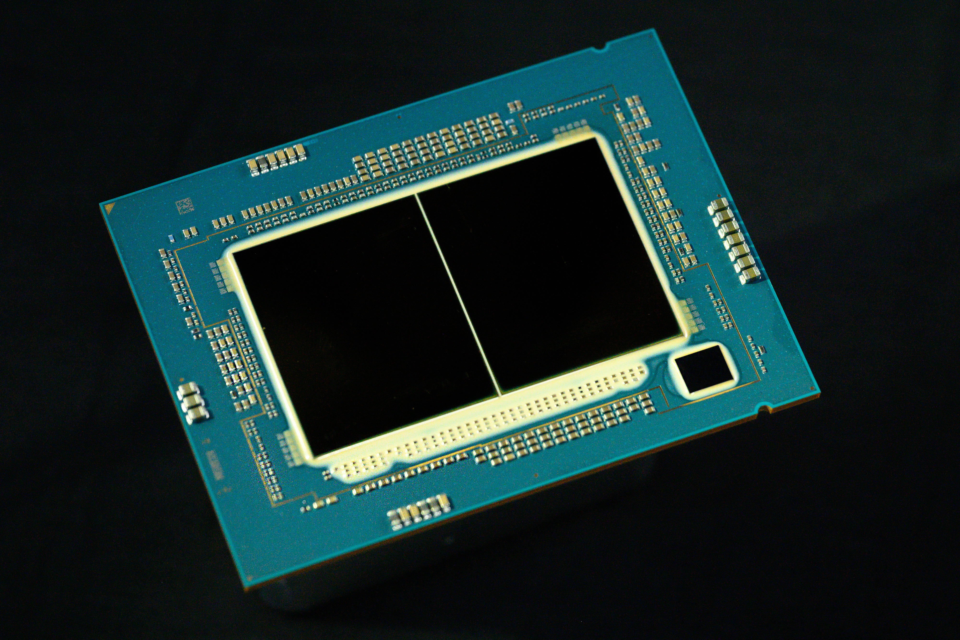
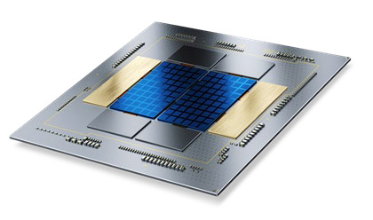
As part of the webinar, Intel also showed off an uncapped Emerald Rapids chip. Based on the sheer amount of silicon on the package and the multi-tile configuration (each tile is easily over 700mm2), we believe this is likely the highest-end XCC configuration. Which at two tiles, is a significant design change from Sapphire Rapids, which used four smaller tiles for its XCC configuration. Which goes to show that even though Sapphire and Emerald are socket-compatible and using the same platform, Intel isn't restraining itself from making changes under the hood (or in this case, under the IHS).
Finally, following in the footsteps of the product naming scheme they’ve used for the last several years now, Intel is officially naming Emerald Rapids as the 5th Generation Xeon scalable family. So expect to see the official name used in place of the code name for the bulk of Intel’s announcements and disclosures going forward.
Granite Rapids: Already Sampling, to Ship In 2024 With MCR DIMM Support
Following Emerald Rapids, in 2024 Intel will be shipping Granite Rapids. This will be Intel’s next-generation P-core based product. Like Emerald, Granite has been previously disclosed by Intel, so today’s announcement is an update on their progress there.
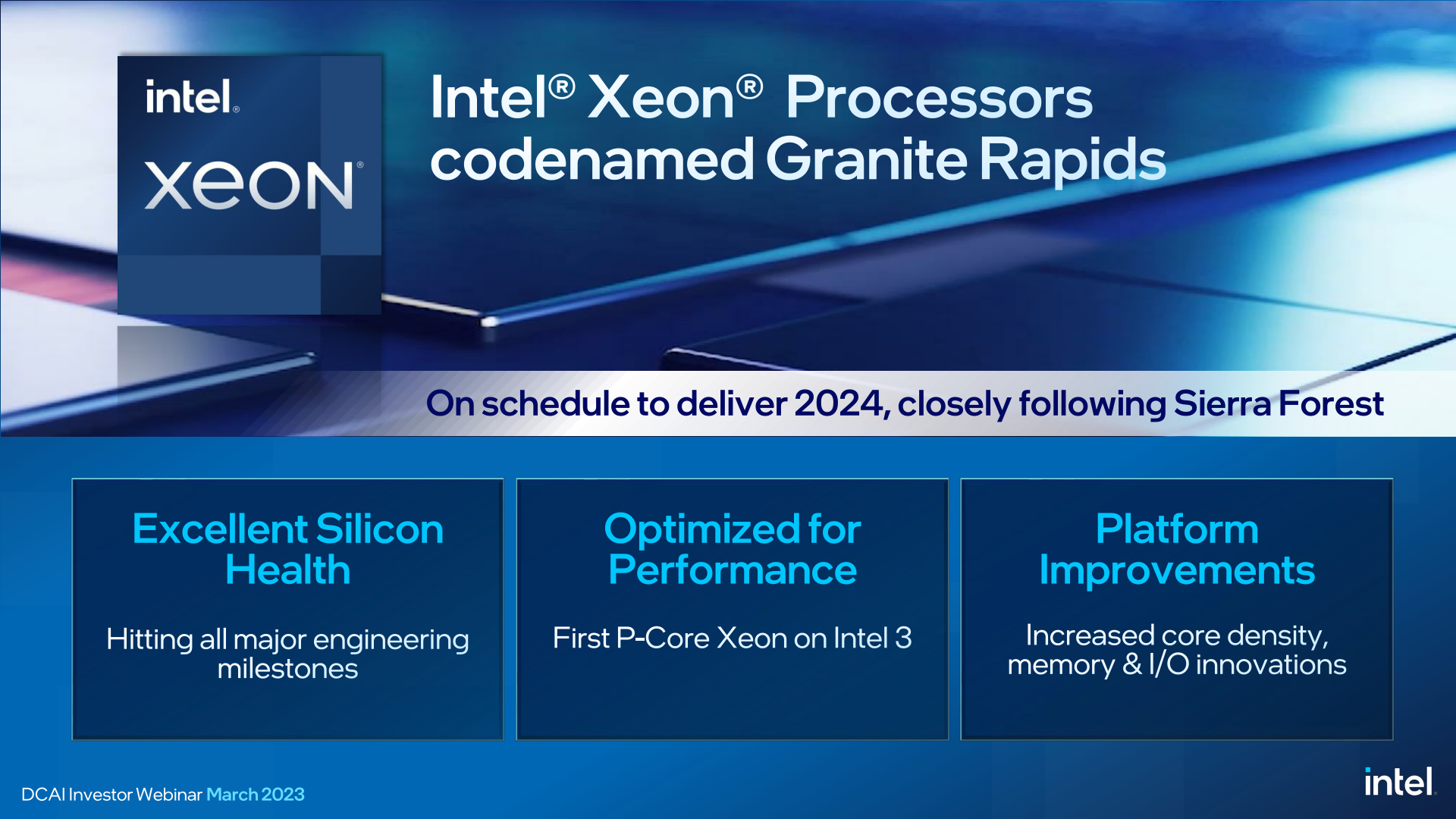
According to Intel, Granite Rapids remains on track for its previously announced 2024 launch. The part is expected to launch “closely following” Sierra Forest, Intel’s first E-core Xeon Scalable processor, which is due in H1’24. Despite being at least a year out, Granite Rapids is already to the point where the first stepping is up and running, and it’s already sampling to some Intel customers.
As noted in previous disclosures, Granite Rapids is a tile-based architecture, with separate compute and I/O tiles – an evolution from Sapphire Rapids, which even in its tiled form is essentially a complete SoC in each tile. Granite Rapids’ compute tiles are being built on the Intel 3 process, Intel’s second-generation EUV node, having been pulled in from Intel 4 in its earliest incarnation. Meanwhile we still don’t have significant official information on the I/O tiles.
Along with upgrades to its CPU architecture, Intel is also disclosing for the first time that Granite Rapids will also come with a notable new memory feature: MCR DIMM support. First revealed by SK hynix late last year, Multiplexer Combined Ranks (MCR) DIMMs essentially gang up two sets/ranks of memory chips in order to double the effective bandwidth to and from the DIMM. With MCR, Intel and SK hynix are aiming to get data rates equivalent to DDR5-8800 (or higher) speeds, which would be a significant boon to memory bandwidth and throughput, as that's often in short supply with today's many-core chips.

As part of today’s presentation, Intel is showing off an early Granite Rapids system using MCR DIMMs to achieve 1.5TB/second of memory bandwidth on a dual socket system. Based on Intel’s presentation, we believe this to be an 8 12 channel memory configuration with each MCR DIMM running at the equivalent of DDR5-8800 speeds.
As an aside, it’s worth noting that as the farthest-out P-core Xeon in Intel’s roadmap, there’s a notable lack of mention of High Bandwidth Memory (HBM) parts. HBM on Sapphire Rapids was used as the basis of Intel’s offerings for the HPC market, and while that wasn’t quite a one-off product, it’s close. Future HPC-focused CPUs were being developed as part of the Falcon Shores project, which was upended with the change to Intel’s GPU schedule. So at this time, there is not a new HBM-equipped Xeon on Intel’s schedule – or at least, not one they want to talk about today.
Sierra Forest: The First E-Core Xeon and Intel 3 Lead Product, Shipping H1’24
Shifting gears, we have Intel’s forthcoming lineup of E-core Xeons. These are chips that will be using density-optimized “efficiency” cores, which were introduced by Intel in late 2021 and have yet to make it to a server product.
Sierra Forest is another previous Intel disclosure that the company is updating investors on, and is perhaps the most important of them. The use of E cores in a Xeon processor will significantly boost the number of CPU cores Intel can offer in a single CPU socket, which the company believes will be extremely important for the market going forward. Not only will the E core design improve overall compute efficiency per socket (for massively threaded workloads, at least), but it will afford cloud service providers the ability to consolidate even more virtual machine instances on to a single physical system.

Like Granite Rapids, Sierra Forest is already up and running at Intel. The company completed the power-on process earlier in the quarter, getting a full operating system up and running within 18 hours. And even though it’s the first E-core Xeon, it’s already stable enough that Intel has it sampling to at least one customer.
As previously disclosed, despite the E-Core/P-Core split, Sierra Forest and Granite Rapids will be sharing a platform. In fact, they’re sharing a whole lot more, as Sierra will also use the same I/O tiles as Granite. This allows Intel to develop a single set of I/O tiles and then essentially swap in E-core or P-core tiles as needed, making for Sierra Forest or Granite Rapids.
And for the first time, we have confirmation of how many E-cores that Sierra will offer. The Xeon will ship with up to 144 E-cores, over twice as many cores as found on today’s P-core based Sapphire Rapids processors. There are no further architectural disclosures on the E-cores themselves – it was previously confirmed that it’s a post-Gracemont architecture – so more details are to come on that front. Gracemont placed its E-cores in quads, which if that holds for the CPU architecture used in Sierra Forest, would mean we’d be looking at 36 E-core clusters across the entire chip.

With Sierra Forest up and running, this also means that Intel has wafers to show off. As part of her portion of the presentation, Lisa Spelman, Intel's CVP and GM of the Xeon product lineup, held up a finished Sierra Forest compute tile wafer to underscore Intel's progress in manufacturing their first E-core Xeon CPU.
Speaking of manufacturing, Intel has also confirmed that Sierra Forest is now the lead product for the Intel 3 node across the entire company. Which means Intel is looking to make a massive leap in a very short period of time with respect to its Xeon product lineup, moving from Intel 7 on Emerald Rapids in Q4’23 to their second-generation EUV process no later than Q2’24. Sierra does get the benefit of products based on Intel 4 (the company’s first-generation EUV process) coming first, but this still makes Sierra’s progress very important, as Intel 3 is the first “full service” EUV process for Intel, offering support for Intel’s complete range of cell libraries.
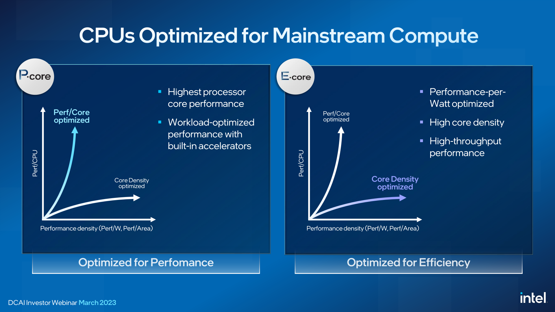
Of all of the Xeon processor architectures outlined today, Sierra is arguably the most important for Intel. Intel’s competitors in the Arm space have been offering high density core designs based on the Neoverse architecture family for a few years now, and arch-rival AMD is going the same direction this year with the planned launch of its Zen 4c architecture and associated EPYC “Bergamo” processors. Intel expects an important subset of their customers to focus on maximizing the number of CPU cores over growing their overall socket counts – thus making data center CPU revenue more closely track core counts than socket counts – so Intel needs to meet those demands while fending off any competitors wanting to do the same.
Clearwater Forest: Second-Gen E-core Xeon In 2025 on Intel 18A Process
Finally, in an all-new disclosure for Intel, we have our first details on the part that will succeed Sierra Forest as Intel’s second-generation E-core Xeon processor. Codenamed Clearwater Forest, the follow-up E-core part is scheduled to be delivered in 2025, placing it no more than 18 months after Sierra Forest.
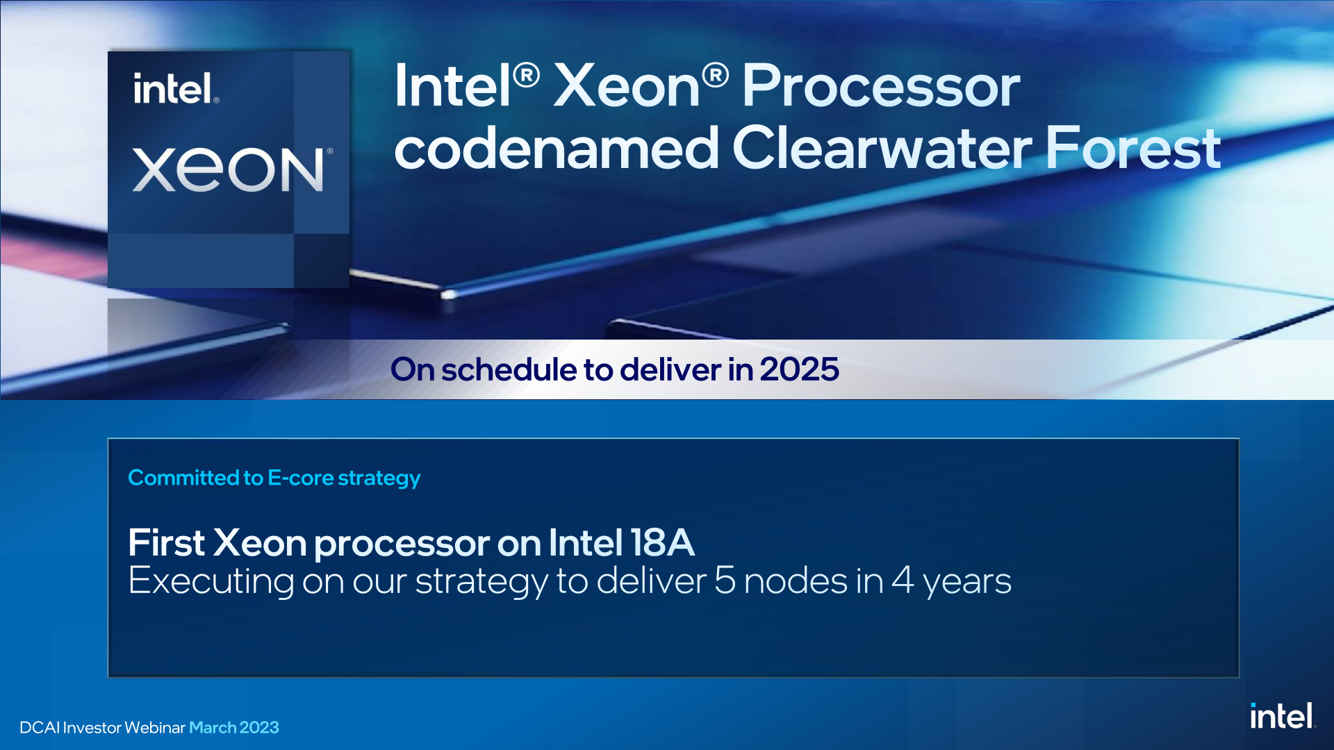
Similar to how Sierra is Intel’s first Intel 3 part, Clearwater Forest is slated to be the first Xeon produced on Intel’s 18A process – their second-generation RibbonFET process, which last year was moved up in Intel’s schedule and will be going into production in the second half of 2024.
At two years out, Intel isn’t disclosing anything else about the chip. But its announcement today is to confirm to investors that Intel is committed to the E-core lineup for the long-haul, as well as to underscore how, on the back of the 18A process, this is the point where Intel expects to re-attain process leadership. Meanwhile, Intel has also confirmed that there won’t be any Xeons made on their early 20A process, so Clearwater Forest will be Intel’s first RibbonFET-based Xeon, period.
Finally, it’s worth noting that with the latest extension to Intel’s CPU roadmap, P-core and E-core Xeons are remaining distinct product lines. Intel has previously commented that their customers either want one core or the other on a CPU – but not both at the same time – and Clearwater Forest maintains this distinction.
| Xeon Scalable Generations | ||||||
| Date | AnandTech | Codename | Abbr. | Max Cores |
Node | Socket |
| Q3 2017 | 1st | Skylake | SKL | 28 | 14nm | LGA 3647 |
| Q2 2019 | 2nd | Cascade Lake | CXL | 28 | 14nm | LGA 3647 |
| Q2 2020 | 3rd | Cooper Lake | CPL | 28 | 14nm | LGA 4189 |
| Q2 2021 | Ice Lake | ICL | 40 | 10nm | LGA 4189 | |
| Q5 2022 | 4th | Sapphire Rapids | SPR | 60 P | Intel 7 | LGA 4677 |
| Q4 2023 | 5th | Emerald Rapids | EMR | >60 P | Intel 7 | LGA 4677 |
| H1'2024 | 6th? | Sierra Forest | SRF | 144 E | Intel 3 | ? |
| 2024 | Granite Rapids | GNR | ? P | Intel 3 | ||
| 2025 | 7th? | Clearwater Forest | CWF | ? E | Intel 18A | ? |
| ? | Next-Gen P | ? | ? P | ? | ||
AI Accelerators & FPGAs: Capturing Market Share At All Ends
While the bulk of today’s presentation from Intel is focused on their CPU roadmap, the company is also briefly touching on the roadmaps for their FPGA and dedicated AI accelerator products.
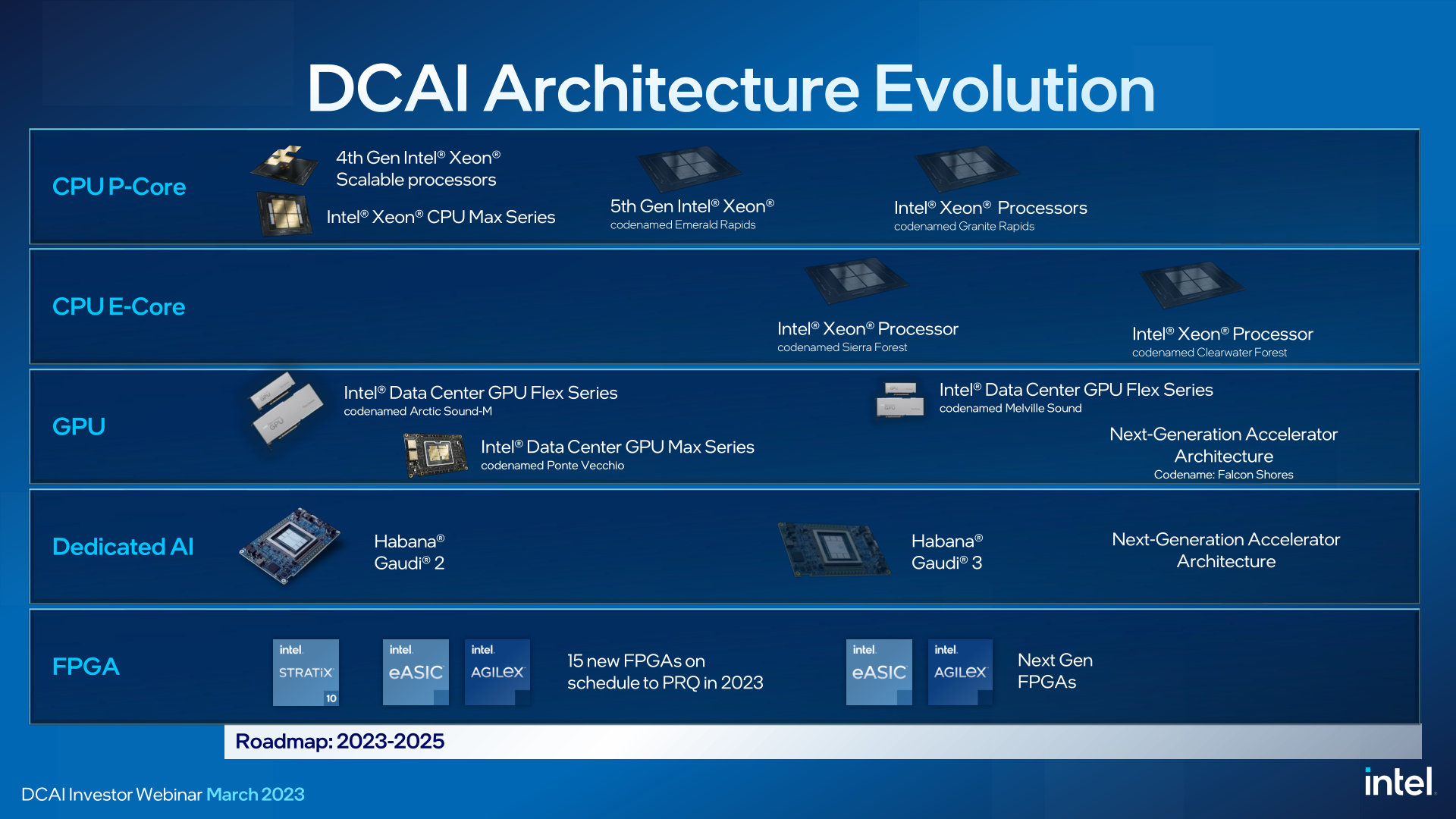
First and foremost, Intel is expecting to qualify (PRQ) 15 new FPGAs across the Stratix, eASIC, and Agilex product lines this year. There are no further technical details on these, but the products, and their successors, are in the works.
Meanwhile, for Intel’s dedicated AI acceleration ASICs, the company’s Habana Labs division has recently tapped-in their next-generation Gaudi3 deep learning accelerator. Gaudi3 is a process shrink of Gaudi2, which was first released back in the spring of 2022, moving from TSMC’s 7nm process to a 5nm process. Intel isn’t attaching a delivery date to the chip for its investor crowd, but more details will be coming later this year.
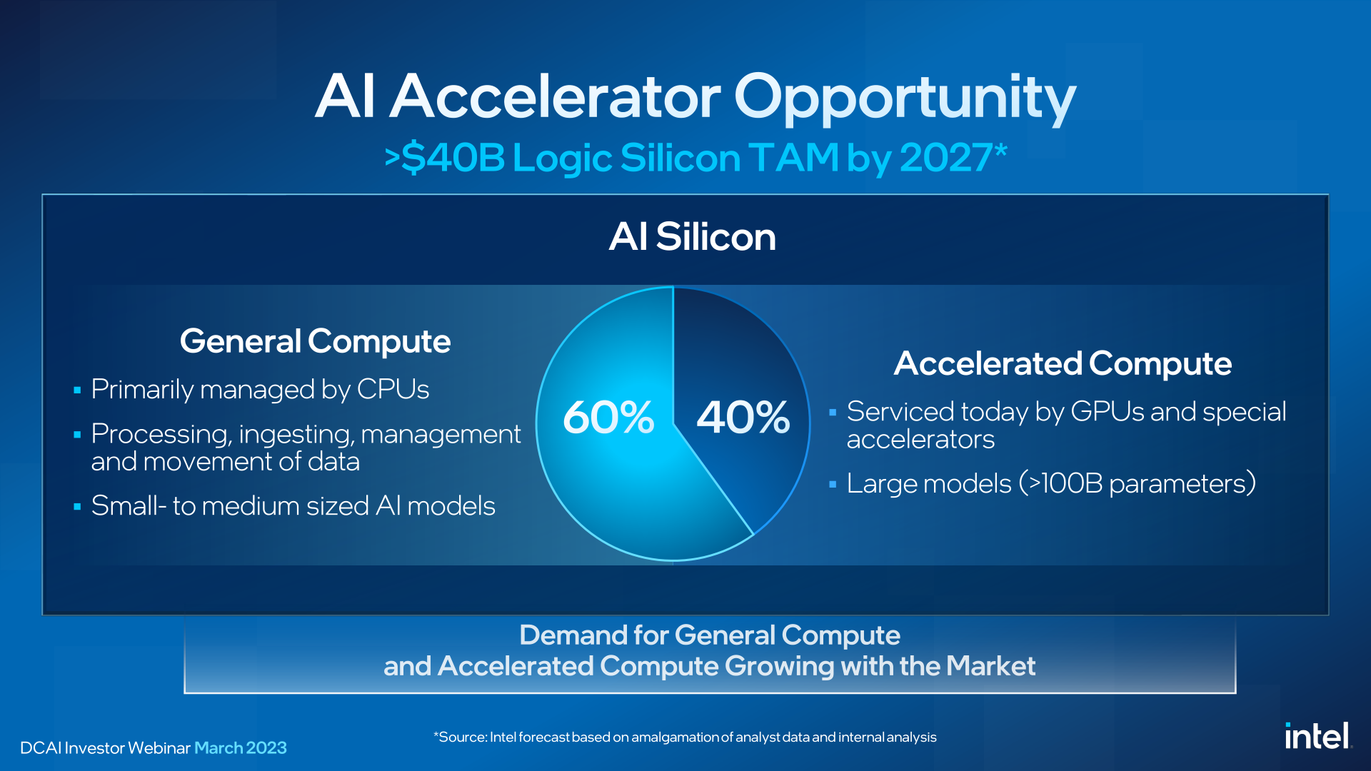
All told, Intel is projecting the market for AI accelerators to be at least a $40 billion market opportunity by 2027. And the company intends to tackle the market from all sides. That means CPUs for AI workloads that are still best served by CPUs (general computer), GPUs and dedicated accelerators for tasks that are best served by highly parallel processors (accelerated computer), and then FPGAs bridging the middle as specialist hardware.
It’s interesting to see that, despite the fact that GPUs and other highly parallel accelerators deliver the best performance on large AI models, Intel doesn’t see the total addressable market for AI silicon being dominated by GPUs. Rather they expect the 2027 market to be a 60/40 split in favor of CPUs, which given Intel’s much stronger position in CPUs than GPUs, would certainly be to their advantage. Certainly, CPUs aren’t going anywhere even for AI workloads (if nothing else, something needs to prepare the data for those GPUs), but it will be interesting to see if Intel’s TAM predictions hold true in 4 years, especially given the eye-watering prices that GPU vendors have been able to charge in recent years.


47 Comments
View All Comments
lemurbutton - Wednesday, March 29, 2023 - link
They're literally releasing 4 new architectures within 1 year. How the hell does that even work? It's confusing as hell to customers. It's a nightmare for vendors. Release one generation, and then 3 months later, release another? Yikes.lemurbutton - Wednesday, March 29, 2023 - link
Also, they're skipping Intel 4 and going straight from Intel 7 to Intel 3. That's a huge jump. Expect delays as usual.Otritus - Wednesday, March 29, 2023 - link
Intel 3 is literally an iteration on Intel 4. It’s like being shocked that Intel went from 14+++ to 10SF for H series mobile. Tiger Lake turned out fine, and as long as there aren’t any issues with Intel 3 or Sierra Forest it’ll turn out fine.name99 - Wednesday, March 29, 2023 - link
Well...- 10SF only worked because it was preceded by a year of failed Canon Lake.
- H Series Mobile wasn't ALSO a completely new design ("Granite Rapids is a tile-based architecture, with separate compute and I/O tiles – an evolution from Sapphire Rapids, which even in its tiled form is essentially a complete SoC in each tile.)
Essentially you're asking us to believe that Intel, which has CONSISTENTLY over-estimated how fast it can iterate - in process, in architecture, and in packaging - will now somehow manage to get all three right. "Sure, right now I can only juggle two balls, and sure I frequently drop one, but hell, let me try three chainsaws, I just *know* I can do it."
Otritus - Wednesday, March 29, 2023 - link
10SF was preceded by 10nm formerly 10nm+ on a year of Ice Lake. Intel 3 will be preceded by Meteor Lake on Intel 4. Intel 3 isn’t a new node, it’s an iteration. Intel 4 is about as delayed as 10nm, and they made a fairly rapid advancement from the working and unexceptional 10+ to the working and good 10SF. I am inclined to believe they can make a similar advancement in a similar time frame from Intel 4 to Intel 3. Leaks indicate that Intel 4 can clock above 4GHz and is a real node, but that Intel may omit a desktop Meteor Lake launch because it would need to be at 5GHz to outperform Raptor Lake.As for packaging, Intel has done Lakefield before which is more advanced than Granite Rapids. Intel should also have Meteor Lake out in 2023 which has the same level of disaggregation as Granite Rapids.
The reason why I am inclined to believe in Sierra Forrest is precisely because it will be reliant upon iterations rather than bringing something entirely new to the table. The only new thing should be the micro architecture. Intel knows how to do IO and IO tiles. They know how to do a 4x10, 5x8, or 6x6 mesh (node count depends on whether or not they will include memory controllers on the CPU tile or IO tile). They know how to do EMIB connections. And, they should have the experience of putting all 3 together this year with Meteor Lake.
mode_13h - Thursday, March 30, 2023 - link
I agree with most of your points, @Otritus. However, I'd take issue with the notion that Meteor Lake is comparable to GNR or even SPR. The main difference is that MTL has all its CPU cores on the same tile. Its tile boundaries all align with what were traditionally all separate chips, if you go back far enough (North Bridge, CPU, GPU, South Bridge), which should significantly reduce the bandwidth requirements and energy-efficiency penalties. For that reason, I regard it as rather conservative.What's interesting and more ambitious about Sapphire Rapids (SPR) is that Intel spanned their mesh interconnect topology over EMIB, almost like it's not even there. Excellent analysis, here:
https://chipsandcheese.com/2023/03/12/a-peek-at-sa...
mode_13h - Thursday, March 30, 2023 - link
> I am inclined to believe in Sierra Forrest is precisely because it will be reliant upon iterationsI've been suspecting the 144-core variant is actually monolithic (aside from the I/O tile, perhaps). If the quad-core tiles are still the same size as a P-core, and we agree it's plausible that you could make a 36-core monolithic tile on Intel 4, then that seems like a good place to start.
The cool thing about showing that wafer is we can estimate the chip sizes. Assuming it's 300 mm in diameter, I get a height of about 20.7 mm and a width of about 20.3 mm. So, that's 420 mm^2 for what I'm guessing are 60 cores (15 dark blobs, which I take to be quad-core clusters). Compare that to the largest SPR die at 770 mm^2 for 34 cores*.
Doing some rough extrapolation, that would make a 144-core die over 1000 mm^2, even before adding any spare clusters for yield. So, I guess the 144 core Sierra Forest is probably comprised of 2 dies of about 80 cores each.
* https://www.angstronomics.com/p/monolithic-sapphir...
Otritus - Thursday, March 30, 2023 - link
Sierra Forrest used e-cores not p-cores. 144 cores is 36 clusters. 1 Gracemont cluster is moderately larger than a Golden/Raptor Cove core. The estimates by size vary, but that would be roughly 40-50 cores in size. When you factor in the significantly increased density of Intel 3, that much is definitely possible as a monolithic design.Another way of looking at it is that the Golden Cove cores took up roughly 2/3 of a Saphire Rapids tile. That’s roughly 17mm2 per core. 48 cores at 17mm2 per core would be 816mm2. Intel 4 roughly doubles density, which would be around 408mm2. Factor in additional space for cache not scaling as well and a larger footprint for the micro architectural enhancements, and you can easily fit 144 cores in less than 600mm2. Locuza on YT had a great breakdown of the Alder Lake die, and Golden Cove server in total takes up around 12-14mm2 rather than the rough 17mm2 I calculated. Monolithic 144C becomes even more reasonable with these numbers.
mode_13h - Friday, March 31, 2023 - link
> Sierra Forrest ... When you factor in the significantly increased density of Intel 3,> that much is definitely possible as a monolithic design.
Yes, this thought experiment is where I started. I worked it out, based on Gracemont figures, although Sierra Forest actually uses Crestmont cores. So, size assumptions based on Gracemont could be well off the mark.
Then, I saw the picture (see article) that purported to be a wafer of SRF dies and that's how I arrived at the estimate of roughly 1000 mm^2 for a monolithic 144 core die. The only way my math is wrong is if that's not 300 mm in diameter, there aren't 60 E-cores on those dies, or that's not even SRF. You see the pic? The caption says it's "a finished Sierra Forest compute tile wafer". Click on it to view full size and count the dies & core clusters for yourself.
We could validate this, if we had a wafer shot of Meteor Lake. Then we should be able to work out the size of a Crestmont cluster on Intel 4.
IanCutress - Wednesday, March 29, 2023 - link
Intel 4 and Intel 20A are going to be client focused